ZHCSGU6A september 2017 – july 2023 ADS8588H
PRODUCTION DATA
- 1
- 1 特性
- 2 应用
- 3 说明
- 4 Revision History
- 5 Pin Configuration and Functions
-
6 Specifications
- 6.1 Absolute Maximum Ratings
- 6.2 ESD Ratings
- 6.3 Recommended Operating Conditions
- 6.4 Thermal Information
- 6.5 Electrical Characteristics
- 6.6 Timing Requirements: CONVST Control
- 6.7 Timing Requirements: Data Read Operation
- 6.8 Timing Requirements: Parallel Data Read Operation, CS and RD Tied Together
- 6.9 Timing Requirements: Parallel Data Read Operation, CS and RD Separate
- 6.10 Timing Requirements: Serial Data Read Operation
- 6.11 Timing Requirements: Byte Mode Data Read Operation
- 6.12 Timing Requirements: Oversampling Mode
- 6.13 Timing Requirements: Exit Standby Mode
- 6.14 Timing Requirements: Exit Shutdown Mode
- 6.15 Switching Characteristics: CONVST Control
- 6.16 Switching Characteristics: Parallel Data Read Operation, CS and RD Tied Together
- 6.17 Switching Characteristics: Parallel Data Read Operation, CS and RD Separate
- 6.18 Switching Characteristics: Serial Data Read Operation
- 6.19 Switching Characteristics: Byte Mode Data Read Operation
- 6.20 Timing Diagrams
- 6.21 Typical Characteristics
-
7 Detailed Description
- 7.1 Overview
- 7.2 Functional Block Diagram
- 7.3 Feature Description
- 7.4
Device Functional Modes
- 7.4.1
Device Interface: Pin Description
- 7.4.1.1 REFSEL (Input)
- 7.4.1.2 RANGE (Input)
- 7.4.1.3 STBY (Input)
- 7.4.1.4 PAR/SER/BYTE SEL (Input)
- 7.4.1.5 CONVSTA, CONVSTB (Input)
- 7.4.1.6 RESET (Input)
- 7.4.1.7 RD/SCLK (Input)
- 7.4.1.8 CS (Input)
- 7.4.1.9 OS[2:0]
- 7.4.1.10 BUSY (Output)
- 7.4.1.11 FRSTDATA (Output)
- 7.4.1.12 DB15/BYTE SEL
- 7.4.1.13 DB14/HBEN
- 7.4.1.14 DB[13:9]
- 7.4.1.15 DB8/DOUTB
- 7.4.1.16 DB7/DOUTA
- 7.4.1.17 DB[6:0]
- 7.4.2 Device Modes of Operation
- 7.4.1
Device Interface: Pin Description
- 8 Application and Implementation
- 9 Device and Documentation Support
- 10Mechanical, Packaging, and Orderable Information
7.3.3 Input Clamp Protection Circuit
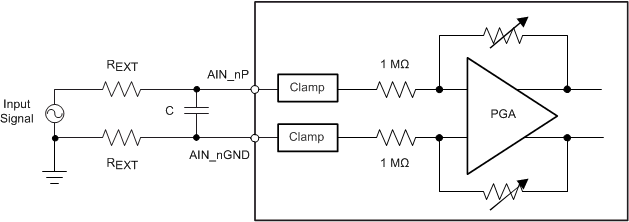
The ADS8588H features an internal clamp protection circuit (as shown in Figure 7-1) on each of the eight analog input channels, respectively. Use of external protection circuits is recommended as a secondary protection scheme to protect the device. Using external protection devices helps with protection against surges, electrostatic discharge (ESD), and electrical fast transient (EFT) conditions.
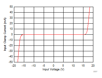
The input clamp protection circuit on the ADS8588H allows each analog input to swing up to a maximum voltage of ±15 V. Beyond an input voltage of ±15 V, the input clamp circuit turns on, still operating off the single 5-V supply. Figure 7-2 illustrates a typical current versus voltage characteristic curve for the input clamp. There is no current flow in the clamp circuit for input voltages up to ±15 V. Beyond this voltage, the input clamp circuit turns on.
 Figure 7-2 I-V Curve for an Input Clamp Protection Circuit (AVDD = 5 V)
For input voltages above the clamp threshold, make sure that input current never exceeds the absolute maximum rating (see the Absolute Maximum Ratings table) of ±10 mA to prevent any damage to the device. A small series resistor placed in series with the analog inputs, as shown in Figure 7-3, is an effective way to limit the input current. In addition to limiting the input current, this resistor can also provide an antialiasing, low-pass filter when coupled with a capacitor. In order to maintain the dc accuracy of the system, matching the external source impedance on the AIN_nP input pin with an equivalent resistance on the AIN_nGND pin is recommended. This matching helps cancel any additional offset error contributed by the external resistance.
 Figure 7-3 Matching Input Resistors on the Analog Inputs of the ADS8588H
The input overvoltage protection clamp on the ADS8588H is intended to control transient excursions on the input pins. Leaving the device in a state such that the clamp circuit is activated for extended periods of time in normal or power-down mode is not recommended because this fault condition can degrade device performance and reliability.