SPRUHW1A June 2014 – October 2021 TMS320F28052-Q1 , TMS320F28052M , TMS320F28052M-Q1 , TMS320F28054-Q1 , TMS320F28054M , TMS320F28054M-Q1
- 1Read This First
- 1 F2805xM InstaSPIN-MOTION Enabled MCUs
- 2InstaSPIN-MOTION Key Capabilities and Benefits
- 3InstaSPIN-MOTION Block Diagrams
- 4Application Examples
- 5Evaluating InstaSPIN-MOTION Performance
- 6Microcontroller Resources
6.7.2 Voltage Reference Connection
Current can flow through the shunt in both positive and negative directions which will create both a positive and negative voltage that is fed back to the shunt amplifier circuit. Most cost-effective motor inverters do not have both positive and negative power supplies that can handle this bipolar signal. A bipolar current signal is brought into an amplifier that will only be effective from zero to the positive voltage supply. To allow the unipolar op-amp circuit to measure a bipolar signal, a voltage reference is summed into the non-inverting side of the current feedback op-amps. The AFE of the 2805x device contains a 6-bit DAC with a voltage follower for providing an output reference for this reason. A circuit configuration that can use a voltage reference to measure the bipolar current signal is shown in Figure 7-6.
 Figure 6-6 Using the AFE's Built-In Voltage Reference For Measuring a Bipolar Signal
Equation 1 shows how to calculate the voltage at VPGA. As an example, set the PGA gain = 3. VADCIN will be 2VBIPOLAR + VREF. Assume the system's VREFHI is 3.3 V. To allow for maximum voltage swing in both directions, VREF is set to 1.65 V. Now the maximum peak VBIPOLAR voltage that can be measure is ±0.825 V.
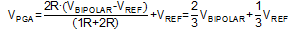
Suppose the same hardware is used and a higher resolution is required. The PGA gain = 6. VADCIN is 4VBIPOLAR + 2VREF. VREF must be adjusted to be 0.825 V. The maximum peak VBIPOLAR voltage that can be measured is ±0.4125 V.
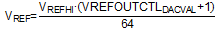
The voltage reference output is adjusted by a 6-bit DAC. The VREFOUTCTL register controls the DAC's voltage output by Equation 2.