SPRUHW1A June 2014 – October 2021 TMS320F28052-Q1 , TMS320F28052M , TMS320F28052M-Q1 , TMS320F28054-Q1 , TMS320F28054M , TMS320F28054M-Q1
- 1Read This First
- 1 F2805xM InstaSPIN-MOTION Enabled MCUs
- 2InstaSPIN-MOTION Key Capabilities and Benefits
- 3InstaSPIN-MOTION Block Diagrams
- 4Application Examples
- 5Evaluating InstaSPIN-MOTION Performance
- 6Microcontroller Resources
6.7.1 Routing Current Signals
Before addressing about the implementation and usage of the PGAs and comparators, it is recommended to consider how current feedback signals are routed from the shunt and then to the input of the PGA. When a shunt resistor is used to measure line current, its value must be small to reduce the amount of power dissipated in the shunt. Because the value is small, so is the resulting voltage drop across the shunt. There is a significant amount of current flowing through the shunt resistors. Copper traces that connect the shunts from the bottom of the power device and then to ground become a resistor in series with the shunt. The parasitic resistance that forms on the copper trace must be taken into consideration when measuring motor line currents with a shunt resistor.
The AFE can have up to three different grounds. The 2805x device has multiple groups of amplifier blocks. Each group of amplifiers has a different ground. M1 ground is used for the group of three PGAs that will feedback three-phase motor currents for this document. For systems with power factor correction, there is another single PGA and its ground is PFC ground. The fixed-gain amplifier block uses M2 ground for its reference and is used in this document for three motor voltage feedbacks.
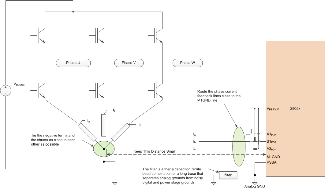
Two options for the feedback of motor shunt current signals to the M1 PGA block of the AFE are discussed. The first option is to use only the internal op-amps for the current feedback as shown in Figure 7-4. All three op-amps share the same ground for the inverting input and therefore a differential signal of the shunt current cannot be created. With single-ended signals, careful layout must be done when grounding the shunts to reduce the amount of differing trace resistance between shunts. It is advised to have the shunt grounds as close together as possible. A trace must run from the point that the shunts come together to the M1gnd pin of the integrated circuit. Because common mode noise can be added to the amplifier, the M1gnd pin and PGA inputs must be made as short as possible. The three phase current traces must be routed as close to the M1gnd trace as possible to reduce the size of the Faraday loop. The Faraday loop is created around the phase current trace that starts from the top of the shunt to the IC and then back on the M1gnd trace to the bottom of the shunt, through the shunt and back to the top of the shunt.
 Figure 6-4 Current Signal Routing Directly to PGAs With
Single-Ended Connections
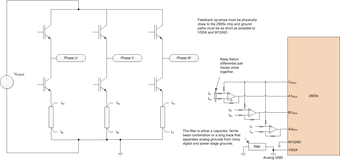
The second, and most noise immune option, is to use external op-amps in a differential amplifier configuration. A true Kelvin connection can feedback directly to the differential amplifier, and then the output of the differential amplifier is sent into the PGA input. Figure 7-5 shows a typical layout when using external differential op-amps. Since the Kelvin connection has low impedance and is a truly differential signal, it provides excellent noise immunity. The external op-amp circuit converts the differential circuit into a single-ended output. The single-ended output is more susceptible to noise and therefore it is best to place the output of the op-amp as close to the AFE input of the processor.
 Figure 6-5 Feedback of Phase Currents Using External
Differential Amplifiers
Why use the PGAs when external amplifiers are already being used? One case would be if many different current rated motors are powered with the same inverter. Amplification of the current signal can be adjusted to best suit the motor size that is controlled. The output of the PGA block is the input of the comparator windows. The PGA still needs to be connected to enable the use of the fault detection circuitry.