SPRADS1 June 2025 F29H850TU
3.1 led_blinky_cpu1.c
This source file within the FOTA_Example_Application project contains the logic required to blink an LED, receive UART commands, and branch back to the flash-based SBL project depending on which UART command is received.
The program begins by initializing the device (clocks, peripheral clocks, interrupts), initializing the Sysconfig settings (UART config, interrupt config) and then enabling interrupts. Once initialization is complete, the device sits in a while loop that waits for a recognized command to be received by the UART module. There is also a CPUTIMER interrupt configured that blinks an LED every second. This acts as the application ISR for the purposes of demonstrating FOTA. Both of these ISRs are configured in the led_blinky_cpu1.syscfg file.
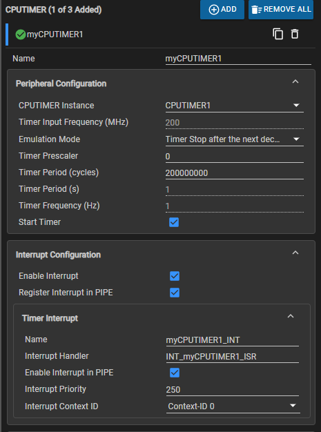
Figure 3-1 shows the configuration of the CPUTIMER interrupt. This is configured with a priority level of 250.
 Figure 3-1 CPU Timer ISR Configuration in
SysConfig
Figure 3-1 CPU Timer ISR Configuration in
SysConfigThe associated ISR is shown in Figure 3-2.
 Figure 3-2 CPU Timer ISR
As shown in Figure 3-3, the UART module is configured with a baud rate of 115200 and triggers an ISR if the RX FIFO receives 8 bytes.
 Figure 3-3 UART Configuration in
SysConfig
Figure 3-3 UART Configuration in
SysConfigThe source code of the UART RX ISR is shown in Figure 3-4.
 Figure 3-4 UART RX ISR
This assigns the command packet variable by reading the UART data and then clear the interrupt flag. Once the command packet has been parsed and assigned to the command variable, the application resumes the while loop in the main function.
 Figure 3-5 Main Loop
Within this main function, the command value is constantly compared to the predefined command packet values in f29h85x_kernel_commands_cpu1.h. These values are common between the flash-based SBL, UART host programmer, and the FOTA_Example_Application. Once a valid command is received, the example project jumps to the appropriate entry point. The macros used in the CPU_jumpToAddr() function can be found at the top of led_blinky_cpu1.c.
 Figure 3-6 Addresses to Branch to in SBL
to Perform FOTA Upgrade
Figure 3-6 Addresses to Branch to in SBL
to Perform FOTA UpgradeThese correspond directly to memory sections created in the flash-based SBL linker cmd files and output sections created in the ex4_uart_sbl.c file.

 Figure 3-7 Linker CMD Memory Sections and
Output Section Creation
Figure 3-7 Linker CMD Memory Sections and
Output Section CreationOnce the FOTA_Example_Application has received a valid command from the host and has branched back to the flash-based SBL project, the application ISRs continue to be serviced. The LED continues blinking for the entirety of the firmware update process. Once the flash-based SBL has completed the firmware upgrade, the device branches back to the FOTA_Example_Application and waits for another command. After a device reset, the banks swap and the newly programmed firmware are in the active address space.