SPRAA99C March 2008 – May 2021 AM3351 , AM3352 , AM3354 , AM3356 , AM3357 , AM3358 , AM3359 , AM4372 , AM4376 , AM4377 , AM4378 , AM4379 , OMAPL138B-EP , TMUX646
1 Introduction
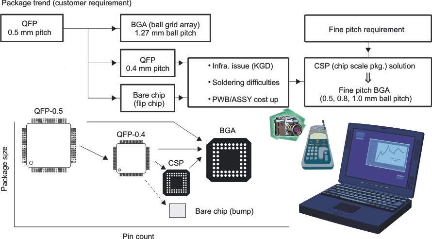
The parallel pursuit of cost reduction and miniaturization in recent years has increased emphasis on very small integrated circuit (IC) package solutions. This is particularly evident in consumer-based end equipment using digital signal processor (DSP) solutions such as wireless telephones, laptop computers, and hard-disk drives. Despite the formal definition, packages with an area similar in size to the IC they encapsulate are loosely referred to as chip scale packages (CSPs). Figure 1-1 illustrates this trend.
 Figure 1-1 Packaging
Trends
Figure 1-1 Packaging
TrendsCSPs are in many ways an ideal solution to the cost reduction and miniaturization requirements. They offer enormous area reductions compared to quad flat packages (QFPs) and have increasing potential to do so without adding to system-level cost. In the best case, CSPs compete today on a cost-per-terminal basis with QFPs. Various CSPs from Texas Instruments (TI) are now available at cost parity with thin QFPs.
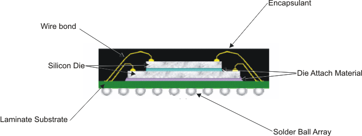
Texas Instruments produces a laminate-based family of CSPs known as New Fine Pitch Ball Grid Array packages (also referred to as nFBGA packages). Like most other CSPs, nFBGA packages use solder alloy balls as the interconnect between the package substrate and the board on which the package is soldered. The nFBGA family comes in a range of solder ball pitch, and can accommodate various stacked die configurations, with as many as three die housed in each package. Figure 1-2 shows the structure of TI’s nFBGA package.
 Figure 1-2 Structure
of TI’s nFBGA Package
Figure 1-2 Structure
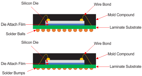
of TI’s nFBGA PackageTI also offers small body nFBGAs for customers looking to reduce the PCB footprint even further. Structure is nearly identical to that of the standard nFBGA shown in Figure 1-2. The major difference is the package thickness. Standard nFBGAs have a thickness of ~1 mm while the small body variants can range from 0.45-1 mm. This is achieved by using a thinner substrate material and die attach film instead of epoxy.
Package stack up can be minimized even further by using solder bumps rather than the standard BGA solder balls. The reduced height of the bumps allows the smallest possible package height while offering exceptional board level reliability performance. Figure 1-3 shows the structure of TI’s small body nFBGAs.
 Figure 1-3 Structure of TI’s Small Body
nFBGA Packages
Figure 1-3 Structure of TI’s Small Body
nFBGA PackagesTexas Instruments addressed several key issues in package assembly to produce a CSP that is not only physically and mechanically stable but cost-effective for a wide variety of applications.
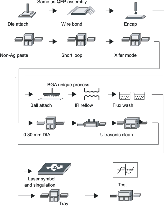
Figure 1-4 shows a general flow used to produce TI nFBGA packages.
 Figure 1-4 nFBGA
Package Assembly Flow
Figure 1-4 nFBGA
Package Assembly FlowThe nFBGA package has been fully qualified in numerous applications and is being used extensively in mobile phones, laptops, modems, handheld devices, and office environment equipment. For more information on using reliable and cost-effective nFBGA packaging in your application, contact your local TI field sales office.