SPRAA99C March   2008  – May 2021 AM3351 , AM3352 , AM3354 , AM3356 , AM3357 , AM3358 , AM3359 , AM4372 , AM4376 , AM4377 , AM4378 , AM4379 , OMAPL138B-EP , TMUX646


  1.   Trademarks
  2. 1Introduction
  3. 2PCB Design Considerations
    1. 2.1 Solder Land Areas
    2. 2.2 Conductor Width/Spacing
    3. 2.3 High-Density Routing Techniques
    4. 2.4 Via Density
    5. 2.5 Conventional PCB Design
    6. 2.6 Advanced Design Methods
  4. 3Reliability
    1. 3.1 Reliability Calculations
    2. 3.2 Package Characteristics
    3. 3.3 Thermal Modeling
  5. 4Surface-Mounting nFBGA Packages
    1. 4.1 Design for Manufacturability (DFM)
    2. 4.2 Solder Paste
    3. 4.3 Solder Ball Collapse
    4. 4.4 Reflow
    5. 4.5 Inspection
  6. 5Packing and Shipping
    1. 5.1 Tray Packing Method
    2. 5.2 Tape-and-Reel Packing Method
    3. 5.3 Tape Format
    4. 5.4 Device Insertion
    5. 5.5 Packaging Method
  7. 6Sockets
    1. 6.1 The Design Challenge
    2. 6.2 Contacting the Ball
    3. 6.3 Pinch Contact
    4. 6.4 Micro Tuning Fork Contact
    5. 6.5 Texas Instruments Sockets
  8. 7Summary
  9.   A Frequently Asked Questions
    1.     A.1 Package Questions
    2.     A.2 Assembly Questions
    3.     A.3 Small Body nFBGA Package Questions
  10.   B Package Data Sheets
  11.   C Thermal Modeling Results
  12.   Revision History

Via Density

Via density, as mentioned earlier, can be a limiting factor when designing high-density boards. Via density is defined as the number of vias in a particular board area. Using smaller vias increases the routability of the board by requiring less board space and increasing via density. The invention of the microvia, shown in Figure 2-5, has solved many of the problems associated with via density.
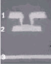
GUID-7BE627A7-C105-4F63-AF06-502C0863260C-low.gifFigure 2-5 Microvia Structure

Microvias are often created using a laser to penetrate the first few layers of dielectric. The laser can penetrate a 4-mil-thick dielectric layer, creating the 4 μm microvia shown in Figure 2-5. The layout designer can now route to the first internal board layer. Two layers (each 4 mils thick) can be laser-drilled, creating a 200 μm microvia diameter. In this case, routing to the first two internal layers is possible.