SPRAA99C March 2008 – May 2021 AM3351 , AM3352 , AM3354 , AM3356 , AM3357 , AM3358 , AM3359 , AM4372 , AM4376 , AM4377 , AM4378 , AM4379 , OMAPL138B-EP , TMUX646
2.1 Solder Land Areas
Designs of both the nFBGA package itself and the printed circuit board (PCB) are important in achieving good manufacturability and optimum reliability. In particular, the diameters of the package vias and the board lands are critical. While the actual sizes of these dimensions are important, their ratio is more critical. Figure 2-1 illustrates the package via-to-PCB configuration and Figure 2-2 illustrates why this ratio is critical.
 Figure 2-1 Package
Via to Board Land Area Configuration
Figure 2-1 Package
Via to Board Land Area Configuration Figure 2-2 Effects
of Via-to-Land Ratios
Figure 2-2 Effects
of Via-to-Land RatiosIn the top view of Figure 2-2, the package via is larger than the PCB via, and the solder ball is prone to crack prematurely at the PCB interface. In the middle view, the PCB via is larger than the package via, which leads to cracks at the package surface. In the bottom view, where the ratio is almost 1:1, the stresses are equalized and neither site is more susceptible to cracking than the other.
Solder lands on the PCB are generally simple round pads. Solder lands are either solder-mask-defined or non-solder-mask-defined.
- Solder-mask-defined (SMD) land. With this method, the copper pad is made larger than the desired land area, and the opening size is defined by the opening in the solder mask material. The advantages normally associated with this technique include more closely controlled size and better copper adhesion to the laminate. Better size control is the result of photo imaging the stencils for masks. The chief disadvantage of this method is that the larger copper spot can make routing more difficult.
- Non-solder-mask-defined (NSMD) land. Here, the land area is etched inside the solder mask area. While the size control is dependent on copper etching and is not as accurate as the solder mask method, the overall pattern registration is dependent on copper artwork, which is quite accurate. The tradeoff is between accurate dot placement and accurate dot size.
For an example of optimum land diameters and configurations for a common nFBGA pitch, see Table 2-1.

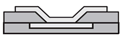 It is not
recommended to use "U" shape PCB land because of trapping void during
reflow.
It is not
recommended to use "U" shape PCB land because of trapping void during
reflow.| All Measurements in mm | Ball Size, SMO, Pad Size and Apertures are Shown in Diameters | |||||
|---|---|---|---|---|---|---|
| Ball Pitch | Solder Mask Type | PCB Design | Stencil Design | Area Aspect Ratio | ||
| SMO | Pad Size | Thickness | Aperture | |||
| 0.4 | SMD | 0.225 | 0.300 | 0.076 | 0.250 | 0.82 |
| NSMD | 0.300 | 0.225 | ||||
| 0.5 | SMD | 0.300 | 0.400 | 0.100 | 0.300 | 0.75 |
| NSMD | 0.400 | 0.300 | ||||
| 0.65 | SMD | 0.350 | 0.450 | 0.127 | 0.350 | 0.69 |
| NSMD | 0.450 | 0.350 | ||||
| 0.8 | SMD | 0.400 | 0.500 | 0.152 | 0.400 | 0.66 |
| NSMD | 0.500 | 0.400 | ||||
| 1 | SMD | 0.450 | 0.550 | 0.152 | 0.450 | 0.74 |
| NSMD | 0.550 | 0.450 | ||||
- Area Ratio = Area of Aperture / Area of Aperture Wall
- For optimal release of solder paste, Area Ratio ≥ 0.66 is recommended.