SPRAA99C March 2008 – May 2021 AM3351 , AM3352 , AM3354 , AM3356 , AM3357 , AM3358 , AM3359 , AM4372 , AM4376 , AM4377 , AM4378 , AM4379 , OMAPL138B-EP , TMUX646
6.3 Pinch Contact
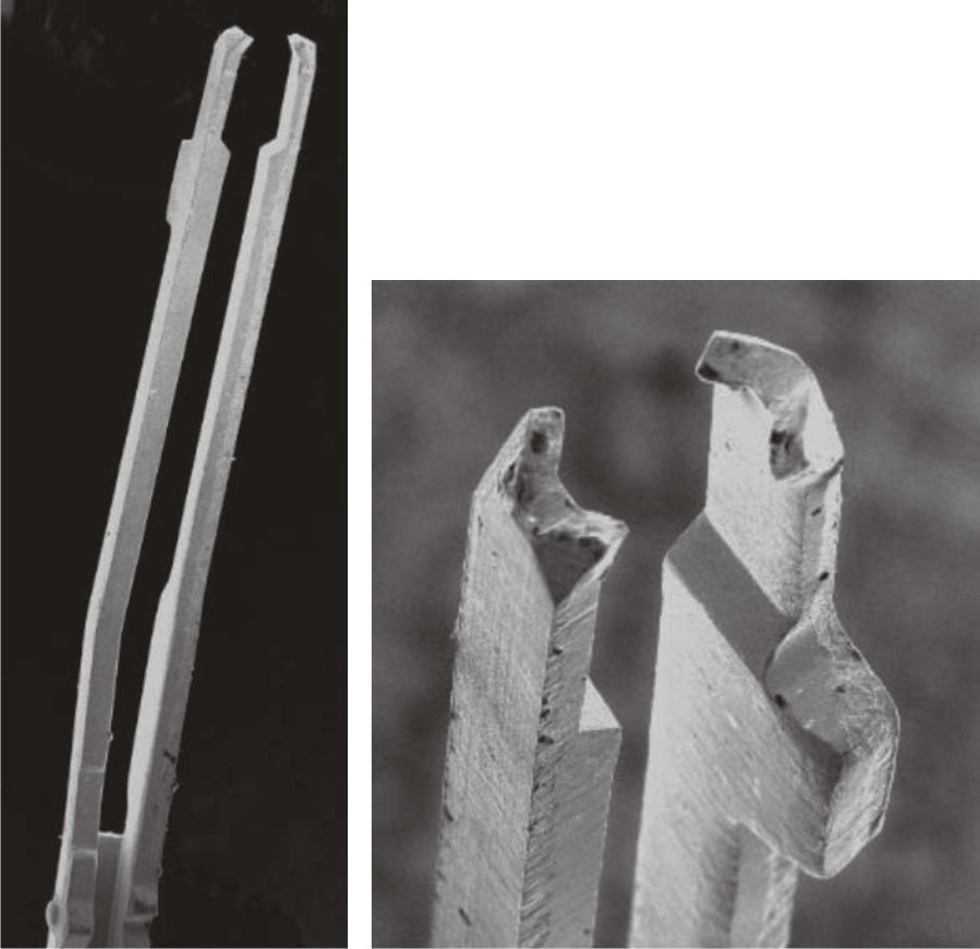
The contact is designed to grip the solder ball with a pinching action. This not only provides electrical contact to the solder ball but also helps retain the package in the socket. The contact is shown in Figure 6-2. It was made using a beryllium copper alloy. This alloy is used for spring applications that are exposed to high stresses and temperatures because of its excellent stress relaxation performance and formability.
 Figure 6-2 Pinch
Contact for Solder Ball
Figure 6-2 Pinch
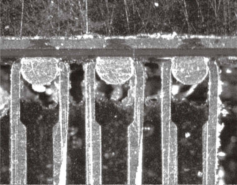
Contact for Solder BallEach contact incorporates two beams that provide an oxide-piercing interface with the sides of the balls above the central area—the equator. No contact is made on the bottom of the solder ball so the original package planarity specifications are unchanged. A photo-micrograph of the contact touching the solder balls is shown in Figure 6-3.
 Figure 6-3 Contact
Area on Solder Ball
Figure 6-3 Contact
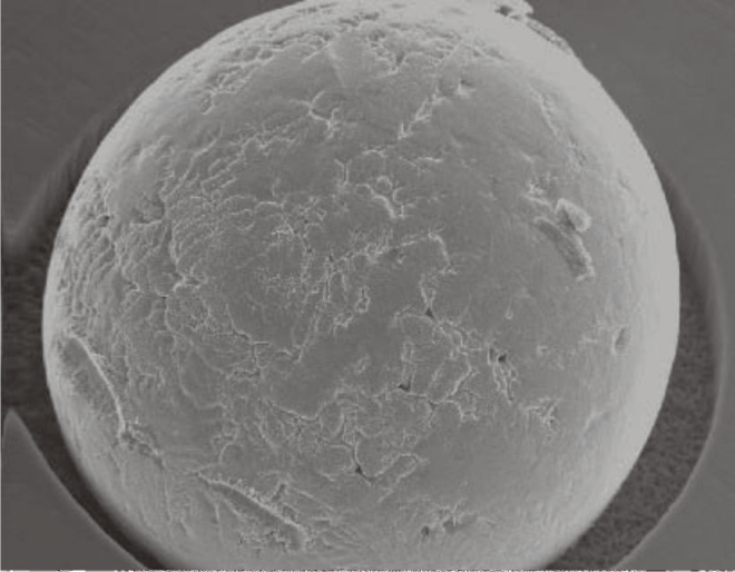
Area on Solder BallThe witness marks left on the solder ball from the contact are shown in Figure 6-4. This ball was contacted at room temperature and it is clear that there was no damage to the bottom of the ball or any witness marks from the contact above the equator.
 Figure 6-4 Witness
Marks on Solder Ball
Figure 6-4 Witness
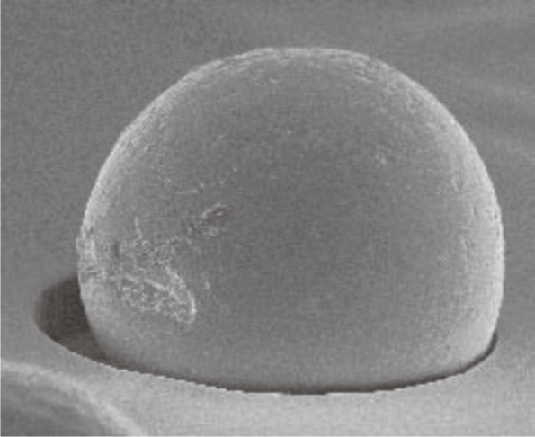
Marks on Solder BallThe effect of burn-in on the probe marks was examined by simulating a cycle and placing a loaded socket into an oven at 125°C for nine hours. The result is shown in Figure 6-5. The penetration of the contact into the solder ball due to the higher temperature is greater but is well within the acceptable range. There was no visible pickup of solder on the contact tips. The location of the contact pinch is clearly seen in this photograph.
 Figure 6-5 Effect of
Bur-In on Probe Mark