SNLU254A November 2020 – July 2022 DS160PT801
3.3 Low-Level Page
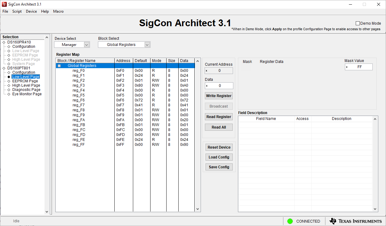
 Figure 3-2 Low-Level Page Screenshot
The Low-Level page of the GUI is used for basic register access to the register map of the DS160PT801 retimer by providing SMBus read and write functions. The ability to save a specific retimer configuration for use later is also provided and can be used performing system evaluation. The description of the input fields of the Low-Level page are as follows.
- Device Select Dropdown allows a user to change the active register map from either the link-width manager or link-width follower SMBus address.
- Block Select Dropdown allows a user to change the active register block between Global, Shared, Channel, or PLL registers.
- Current Address Field displays the currently selected register address.
- Data Field displays the data currently stored at the selected register address.
- Mask Value Field displays the mask value that will be used for write operations at this register. Only the bits that are set to a "1" in this field will be written to.
- Write Register Button issues an SMBus write of the data listed in the data field at the current address using the bit mask indicated in the Mask Value field.
- Broadcast Button becomes active when one of the channel register blocks are selected. Clicking this button performs a write operation similar to the Write Register button, but it will broadcast the write to all channels in the currently selected device.
- Read Register Button issues an SMBus read of the data listed in the current address field.
- Read All Button issues a SMBus read of all registers for the currently selected register block.
- Reset Device Button resets all register values back to their default values. This will cause an active PCIe link to fail.
- Load Config Button can be used to load a previously saved set of SMBus register values.
- Save Config Button saves a file that stores the current values for all SBMus registers. This file can later be loaded using the Load Config button.