SNLU254A November   2020  – July 2022 DS160PT801


  1.   Abstract
  2.   Trademarks
  3. 1EVM Control and Configuration Information
    1. 1.1 Retimer Pin Controls
    2. 1.2 USB-to-SMBus Interface
    3. 1.3 PCIe PRSNT# Signal Control and Configuration
    4. 1.4 PCIe Reference Clock Control and Configuration
  4. 2EVM Power
    1. 2.1 EVM Current Sensing
  5. 3SigCon Architect GUI
    1. 3.1 Setup and Installation
    2. 3.2 Configuration Page
    3. 3.3 Low-Level Page
    4. 3.4 EEPROM Page
    5. 3.5 Control Panel
    6. 3.6 High-Level Page
    7. 3.7 Diagnostic Page
    8. 3.8 Eye Monitor Page
  6. 4PCB Material Information
    1. 4.1 DS160PT801 PCB Design
    2. 4.2 DS160PT801 PCB Stackup
    3. 4.3 DS160PT801 PCB Power Distribution
    4. 4.4 DS160PT801 Local Decoupling
  7. 5DS160PT801X16EVM Schematic
  8. 6Hardware BOM
  9. 7Revision History

DS160PT801 Local Decoupling

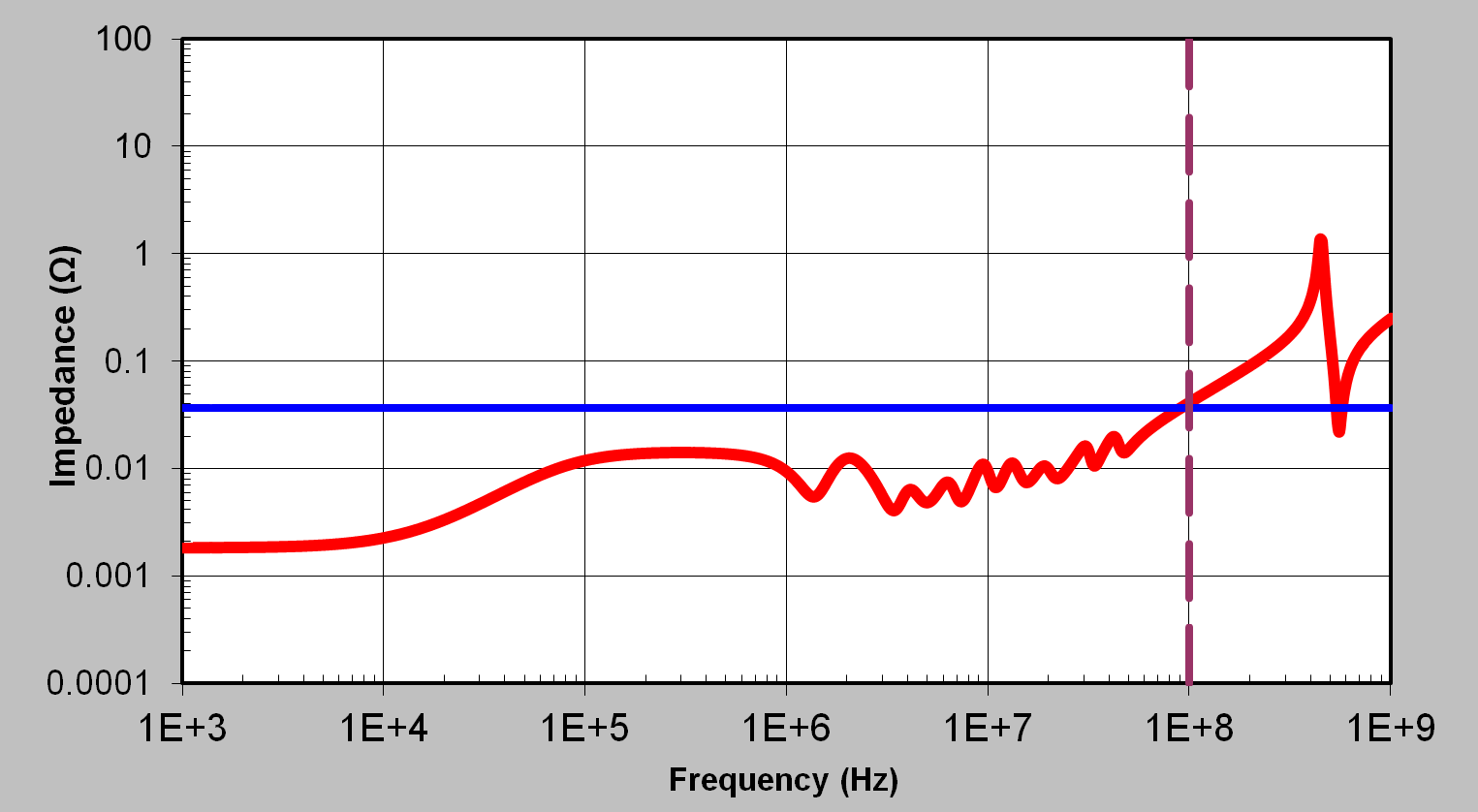
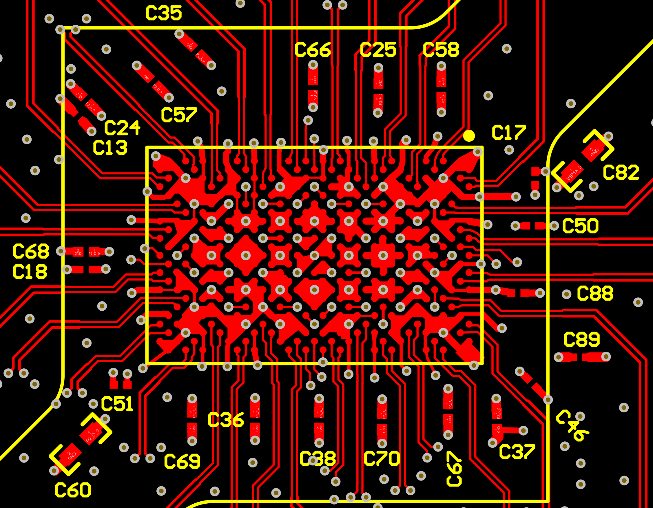
To complement the PCB power layers, decoupling capacitors have been arranged to filter device noise. The design of the high-current analog and digital decoupling uses Top and Bottom layer capacitors to optimize the overall frequency response of the decoupling solution.

GUID-20201025-CA0I-2ZBG-JC8S-BW8S9LSD94SM-low.png

Figure 4-5 Decoupling Solution Frequency Response

Extending the targeted frequency range out to 100 MHz ensures digital noise associated with the PCIe reference clock is minimized. The highest frequency components require very low inductance to perform well. Placing the high current supplies close to the top layer surface ensures the lowest inductance possible to the supply plane and ultimately to the device itself.

GUID-20201025-CA0I-Z9SH-JKLB-NWV0RG5TR7XG-low.png

Figure 4-6 PCB Top Layer