SNLU254A November 2020 – July 2022 DS160PT801
4.3 DS160PT801 PCB Power Distribution
The riser card power distribution network was designed for observation and performance. Four power layers were dedicated to retimer supply voltages. This improves isolation between sensitive analog circuits and reduces losses where high dynamic currents are present.
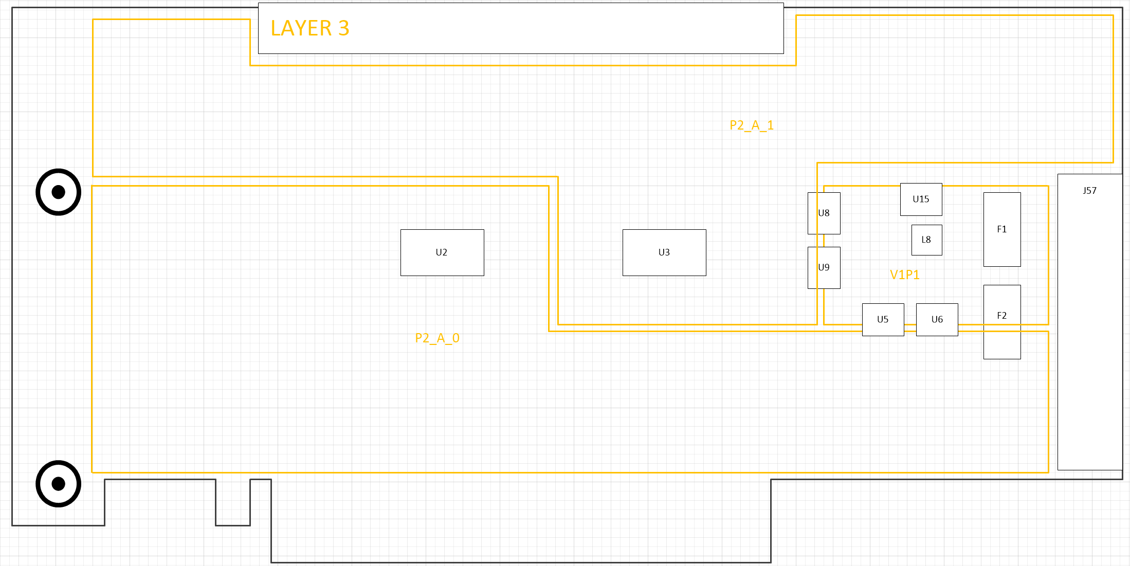
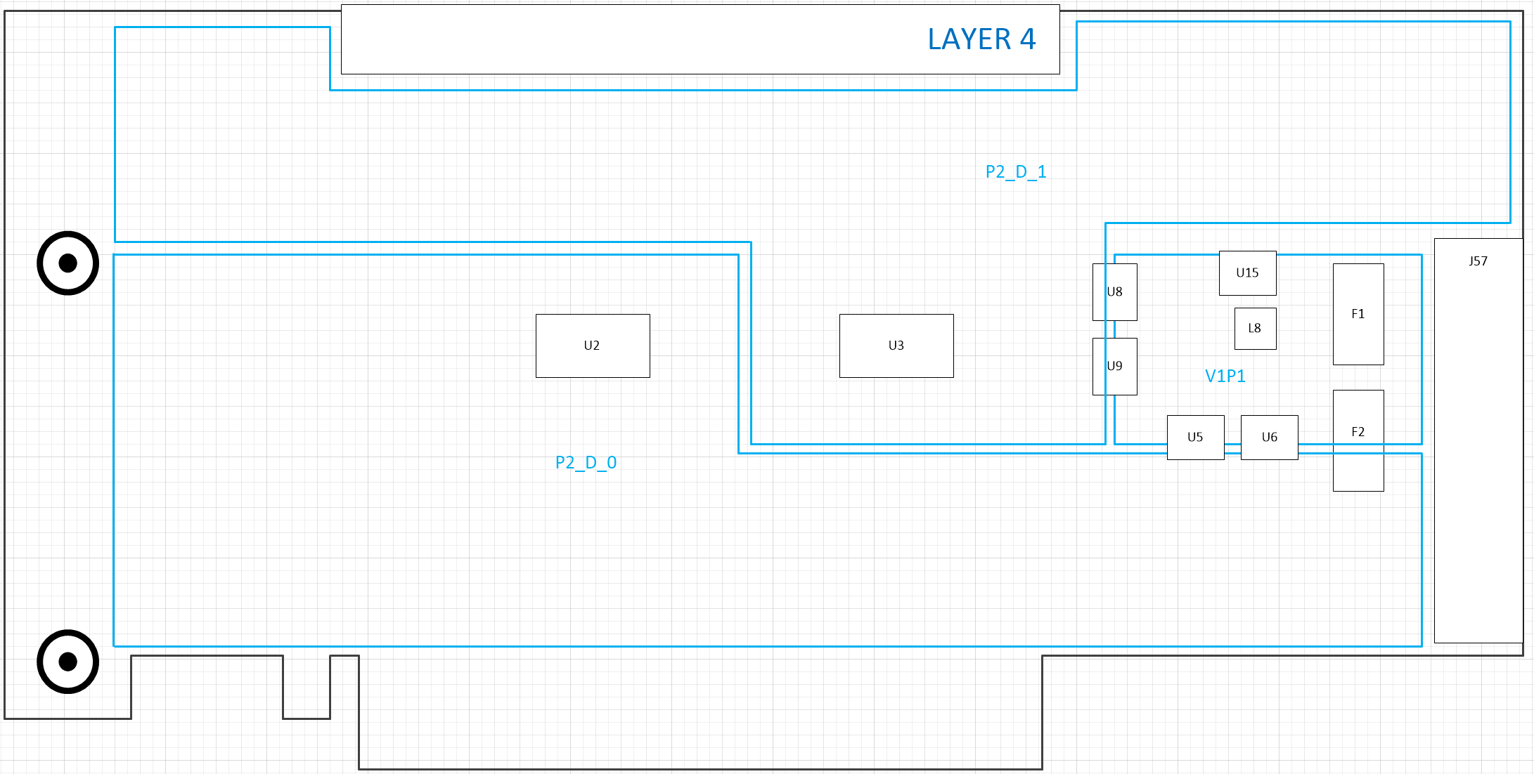
Layer 3 and Layer 4 in the stackup are dedicated to the high-speed analog and digital supply rails. Both of these rails are nominally 1.1-V voltage levels. Using two layers as close to the mounted DS160PT801 as possible improves decoupling performance and aligns with internal package power supply design. Note that previous designs with a single PWR2_HSD supply are completely compatible with the Revision C pre-production silicon used on this EVM.

Figure 4-2 Layer 3 High-Speed Analog Analog Power Rails

Figure 4-3 Layer 4 Digital Power Rails
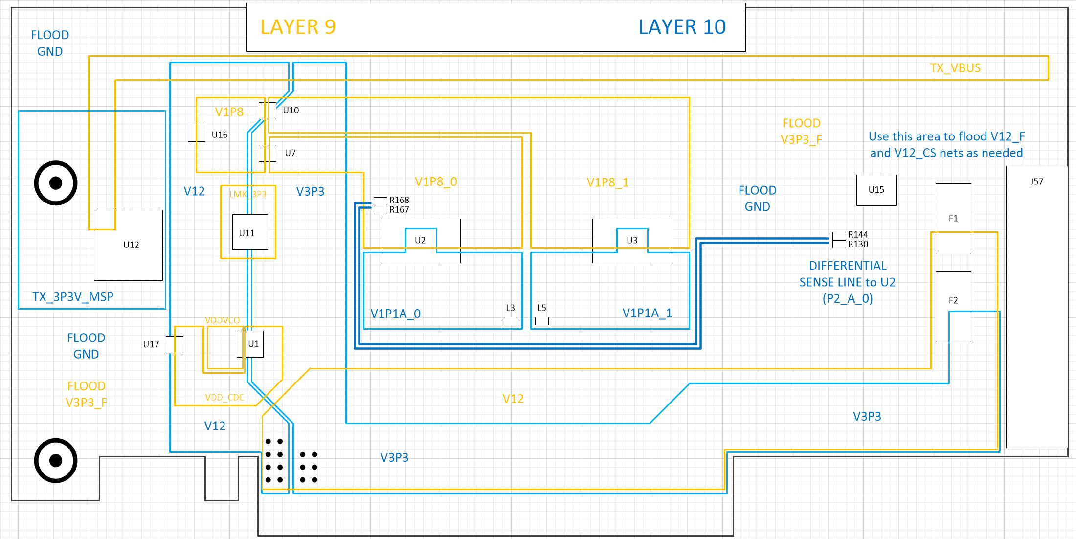
Layer 9 and Layer 10 are used to supply the analog voltages. These retimer supplies are lower current and have relatively constant demand so placements lower in the PCB stackup match their requirements. In addition to retimer supply needs, these layers are also used to provide 3-V and 12-V levels to the attached endpoint and regulator inputs.
As with any Serdes, hardware design power distribution is important to the overall device performance. To ensure optimal voltage levels at the retimer devices, the main 1.1-V regulator uses a remote sense line directly to the U2 retimer. This helps to compensate for any losses on the PCB between the regulator and the device load.

Figure 4-4 Layer 9 and 10 Power Distribution