SLVAF52B July 2021 – November 2021 AFE8092 , TPS62913
2.2 AFE80xx Supply Settling and EVM for TDD Operations
In TDD mode operation Transmit (TX) and Receive (RX) signals are time multiplexed to operate in same frequency spectrum. The time multiplexing is done as per definition of wireless interface standard.
For defined guard period as per the wireless standard interface between TX and RX switching the DAC supply undergoes load transient which results into overshoot and undershoot ripple. If supply rail is not settled before data is transmitted from AFE TX channel, constellation points will be affected, resulting in poor first symbol EVM.
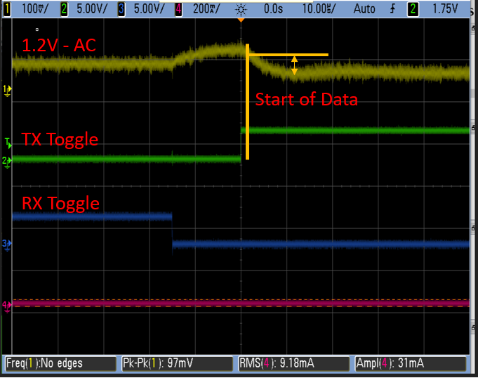
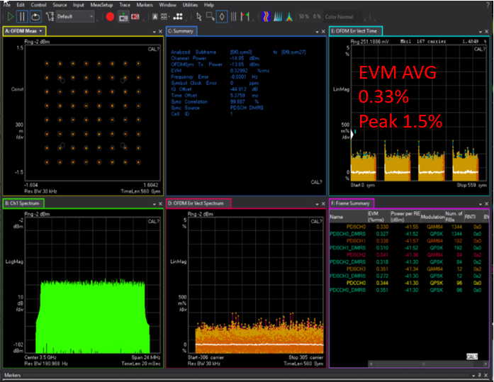
5G NR TDD 20 MHz, 256.76 MSPS data is transmitted from TX channel with 15-us guard period with RX channel. The hardware data delay of start of pulse and actual start of data is 2.5 us. As 1.2-V DAC supply is not settled at 2.5 us, the first symbol is degraded causing EVM peak around 1.5%.
 Figure 2-5 1.2-V Supply
Settling
 Figure 2-6 5G NR TDD EVM
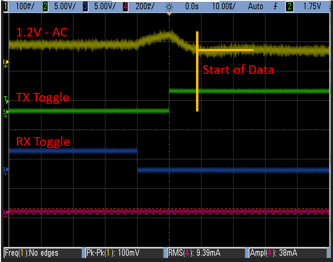
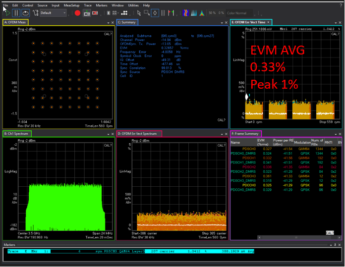
5G NR TDD 20 MHz, 256.76 MSPS data is transmitted from TX channel with 10-us guard period with RX channel. The hardware data delay of start of pulse and data is 7 us. As 1.2-V DAC supply is settled at 7 us, hence the first symbol is not degraded showing EVM peak improvement from 1.5% to 1.0%.
In the above example 1.2-V DC is settled approximately to 96% of final steady state of DC supply at start of data thus preventing degradation of first symbol EVM.
To achieve optimized settling of 1.2-V DC rail for load transient, it is necessary to design Buck converter power stage and secondary closed loop L-C filter with good phase margin and settling response.
TI SWIFTTM based DC-DC power device operating in Advanced Current Mode (ACM) control and optimized power stage helps to achieve AFE80xx supply requirements.
 Figure 2-7 1.2-V Supply
Settling
 Figure 2-8 5G NR TDD EVM