SLVAF10 March 2021 TPS1H000-Q1 , TPS1H100-Q1 , TPS1H200A-Q1 , TPS1HA08-Q1 , TPS1HB08-Q1 , TPS1HB16-Q1 , TPS1HB35-Q1 , TPS1HB50-Q1 , TPS2H000-Q1 , TPS2H160-Q1 , TPS2HB16-Q1 , TPS2HB35-Q1 , TPS2HB50-Q1 , TPS4H000-Q1 , TPS4H160-Q1
4.1.1 Analog Current Sense
Integrated analog current sense functionality allows the device to measure and feedback operating parameters including load current. High accuracy and fast response of the analog sense circuit enables closed-loop control of the high side switch. TPS1AH08-Q1 is one HSS that offers analog sense output that can measure supply voltage, output current, and IC temperature, and will be used as an example in this section.
The analog sense circuit converts its measured parameter into a current according to the specified transfer function. The transfer function of TPS1HA08 is shown in Table 4-1.
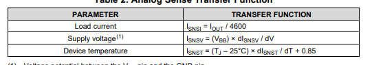 |
For TPS1HA08-Q1, the analog sense outputs a current ISNSFH ~7 mA when there is a fault detected. Device specifications for TPS1HA08-Q1 set the maximum steady-state output current at 10 A, though the analog sense is capable of measuring current higher than this. SNS output value should be clamped (e.g. by Zener diode) to avoid exceeding the input range of the ADC if output current of the high side switch jumps unexpectedly.

Adapted from TPS1HA08 data sheet
In a example application, the designer needs the ability to collect current, voltage, and temperature measurements. This fictitious engineer targets 50-mA output current resolution. The supply voltage for logic is 3.3 V, so AVDD 3.3-V supply is assumed for the converter as well. The system limits along with the corresponding sense currents are listed.
- Peak output current: IOUT = 5 A, ISNS = 1.10 mA
- Peak Temp: Tj=150°C, ISNS = 2.25 mA
- Peak Supply Voltage: Vvs = 15 V, ISNS = 1.29 mA
- SNS Fault current: ISNSFH = 6.9 mA
 Figure 4-2 ADC Range Allocation
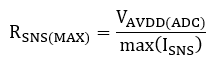
We can determine the maximum feasible value of Rsns possible based on the input range of the ADC and the SNS fault current, which is the absolute maximum. In order to minimize the resolution, the max SNS voltage range is set 10% under the input range of the single-ended ADC and a Zener clamps the fault current ISNSFH to 3.3 V. Without the Zener, the ADC could be damaged as the input voltage would far exceed the device limits. The 300-mV difference allows plenty of headroom to prevent false fault detection.
The analog sense output is gated by both EN and DIAG_EN. The requirement of DIAG_EN allows a controller to multiplex analog sense outputs from several HSS onto a single ADC. After a rising edge of EN, the sense output current, ISNS, settles after a certain time. For TPS1HA08, the maximum settling time of ISNS is 180 µs. Since PWM operation implies that EN is constantly driven high or low, the sense settling time affects every switching cycle ON period where diagnostics are enabled.
A low pass is recommend to filter transients or interference on the analog sense output voltage. In TPS1AH08-Q1, a 10 - 15-kΩ resistor RPROT is suggested to protect the HSS pins. Together with filter capacitor, CSNS , the RC filter is formed. If there is a long lead or trace from the HSS sense pin to the ADC input, the sense resistor and RC filter should be placed close to the ADC prevent interference.
The transfer function of the sense current to the voltage at the ADC input is
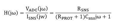
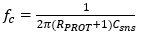
For example, if operating at 1-kHz PWM frequency, we can find a suitable CSNS value for a fixed RPROT of 10 kΩ. By using a rule of thumb we set our target cutoff frequency for the LPF at fc ≥ 10· fPWM. From there,