SLVAF10 March 2021 TPS1H000-Q1 , TPS1H100-Q1 , TPS1H200A-Q1 , TPS1HA08-Q1 , TPS1HB08-Q1 , TPS1HB16-Q1 , TPS1HB35-Q1 , TPS1HB50-Q1 , TPS2H000-Q1 , TPS2H160-Q1 , TPS2HB16-Q1 , TPS2HB35-Q1 , TPS2HB50-Q1 , TPS4H000-Q1 , TPS4H160-Q1
3.3.1 Timing Impact of Finite Slew Rate and Slew Rate Mismatch
If slew rate on/off matching is provided in the data sheet, as it is for TPS1H100-Q1, we can consider the worst-case impact on pulse width from both propagation delay mismatch and slew-rate mismatch. If we consider pulse-width as the duration from the rising and falling edges taken at 50% of max value we get:
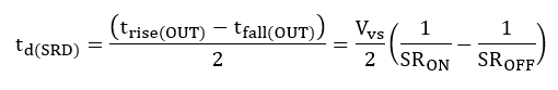
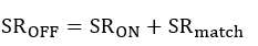
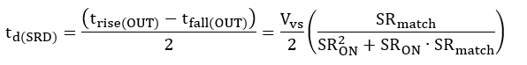
where SRmatch could be positive or negative. If we consider both slew-rate and propagation-delay mismatch, the output pulse-width expression follows:

To illustrate the effect, we use specification of TPS1H100-Q1 and Equation 24 to understand the slew-rate mismatch relationship with PWM accuracy.
- HSS supply voltage: Vvs=10 V and 40 V
- Pulse-width distortion: td(PWD) = ±50 μs (TPS1H100 min/max spec)
- ON Slew rate: SRON = 0.36 V/μs
- Slew rate matching: SRmatch = 0.15 V/μs
- Duty cycle: DIN = 50%
 Figure 3-7 Input-to-Output PW Accuracy Over
Supply Voltage, Considering Slew Rate and Delay Mismatch
Figure 3-7 Input-to-Output PW Accuracy Over
Supply Voltage, Considering Slew Rate and Delay MismatchClearly, if we consider both PWD and slew rate mismatch this places additional limits on feasible PWM frequency especially at higher supply voltages. It is important to note that each high side switch can have varying switching characteristics. Refer to the device parameters and calculation methods above to determine if a specific set of PWM loading conditions is feasible for a selected high side switch.