SLVAF10 March 2021 TPS1H000-Q1 , TPS1H100-Q1 , TPS1H200A-Q1 , TPS1HA08-Q1 , TPS1HB08-Q1 , TPS1HB16-Q1 , TPS1HB35-Q1 , TPS1HB50-Q1 , TPS2H000-Q1 , TPS2H160-Q1 , TPS2HB16-Q1 , TPS2HB35-Q1 , TPS2HB50-Q1 , TPS4H000-Q1 , TPS4H160-Q1
4.3 Side-Stepping Frequency Limitations
In some applications, systems may need to operate at PWM frequencies beyond the 1-2 kHz which most HSS are limited to, but still maintain the robust diagnostics and protection features of a high side switch.
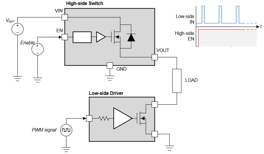
This can be accomplished by reassigning the PWM switching duties from the HSS to a separate low-side switch, such as ULN2003A, which is capable of much higher-frequency operation. For higher-current applications, N-ch FET based low-side driver such as DRV103 may be used. This topology is shown in Figure 4-3. With this dual-IC strategy, a designer still must consider frequency dependent power dissipation and thermals in the HSS, but not HSS switching losses.
 Figure 4-3 Dual-Driver Strategy for
High Frequency PWM