SLUUCC3 february 2021
- 1
- Abstract
- Trademarks
- General Texas Instruments High Voltage Evaluation (TI HV EVM) User Safety Guidelines
- 1General Description
- 2Theory of Operation
- 3Connectors
- 4Quick Start Guide
- 5Physical Dimensions
- 6BQ79631-Q1 EVM Schematic, Assembly, Layout, and BOM
3.3.5 Buffers
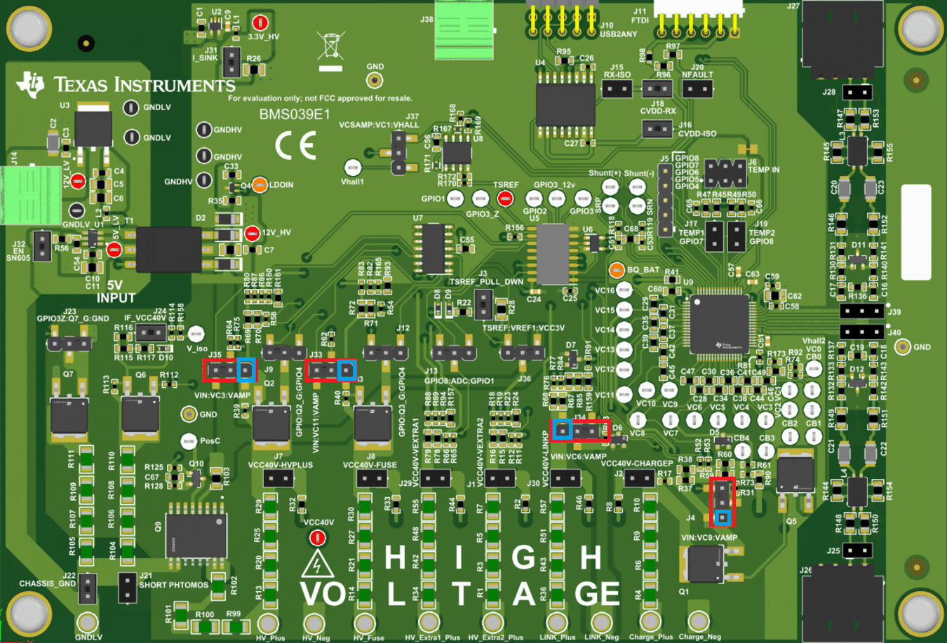
Prior to the VC measurements in the positive side of each high voltage network (not HV_Extra1_Plus or HV_Extra2_Plus), there is a buffer present to prevent leakage current from flowing back into VC pins. This leakage current creates inaccuracy in the measurements made by the VC pins. While TI recommends that these buffers are implemented in the user’s final design for accuracy, if the user wishes to assess impact on accuracy without the buffer, the user can connect to the first pin of the jumper associated with each buffer as shown below. Simply compare the measurement obtained by connecting a DMM to the desired jumper and GNDHV with the measurement seen on the VC pin associated with that network to calculate the percent error that is introduced if a buffer were not to be included in the user’s final design.
 Figure 3-5 Buffer Bypass Jumpers
| Jumper | Network |
|---|---|
| J35 | HV_Plus |
| J33 | HV_Fuse |
| J34 | LINK_Plus |
| J4 | Charge_Plus |