SLUUCC3 february 2021
- 1
- Abstract
- Trademarks
- General Texas Instruments High Voltage Evaluation (TI HV EVM) User Safety Guidelines
- 1General Description
- 2Theory of Operation
- 3Connectors
- 4Quick Start Guide
- 5Physical Dimensions
- 6BQ79631-Q1 EVM Schematic, Assembly, Layout, and BOM
3.3.6 Insulation Detection Network
The insulation detection network on the BQ79631EVM located around HV_plus allows the user to verify that all high voltage networks within their design are properly insulated from low voltage ground. To utilize this feature, first make sure that GPIO2, and GPIO3 are both configured as output high and that GPIO1 is set to ADC only input. Next, connect the desired high voltage at either HV_Plus or at VCC40V. If the user is utilizing the VCC40V supply method, then be sure to place a shunt on the J7 jumper in the same method, as mentioned in Section 3.3.3 to connect the network to the 40-V supply. Additionally, for 40-V connection verify that the J24 jumper is depopulated. This adds increased resistance to the bottom side of the network that makes sure the measurement stays accurate.
To test this feature, simply switch GPIO3 from Output High to Output Low every 5-10 seconds. This connects/disconnects the high voltage supply through the Q9 photoMOS. Measurements are then taken at GPIO1 under both conditions to make sure that the device is properly insulated. The CB1 pin can also be used in place of the GPIO1 pin if the user wishes to utilize this GPIO pin for another purpose.
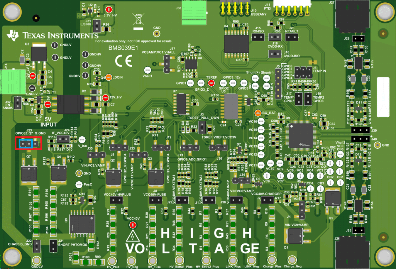
If additional accuracy is required, then the user can utilize the Q7 switch by populating pins 1-2 on J23 shown below. This switch is controlled by an inverted GPIO3 signal so that the Q7 FET switches opposite to the Q9 photoMOS. This introduces no delay in the system and is simply an option available to the user to implement in their design.
 Figure 3-6 Additional FET Option