SLUUCC3 february 2021
- 1
- Abstract
- Trademarks
- General Texas Instruments High Voltage Evaluation (TI HV EVM) User Safety Guidelines
- 1General Description
- 2Theory of Operation
- 3Connectors
- 4Quick Start Guide
- 5Physical Dimensions
- 6BQ79631-Q1 EVM Schematic, Assembly, Layout, and BOM
3.2.3 High-Side and Low-Side Communications
There are two sets of 4-position molex connectors available on each BQ79631EVM board. These provide high-side (J27) and low-side (J26) communications between stacked EVM devices.
| Pin | Name | Comments |
|---|---|---|
| 1 | COML_N | COM low-side negative |
| 2 | COML_P | COM low-side positive |
| 3 | N/A | Unused |
| 4 | N/A | Unused |
| Pin | Name | Comments |
|---|---|---|
| 1 | N/A | Unused |
| 2 | N/A | Unused |
| 3 | COMH_P | COM high-side positive |
| 4 | COMH_N | COM high-side negative |
Isolation Options
Capacitor Only
If the user wishes to utilize the cap only method, no extra modifications need to be made to the EVM since this is the default configuration.
Capacitor and Choke
For the cap and choke method to be implemented, the user must de-solder the R144, R145, R155 and R154 resistors so that the L4 and L3 chokes are not bypassed.
Transformer
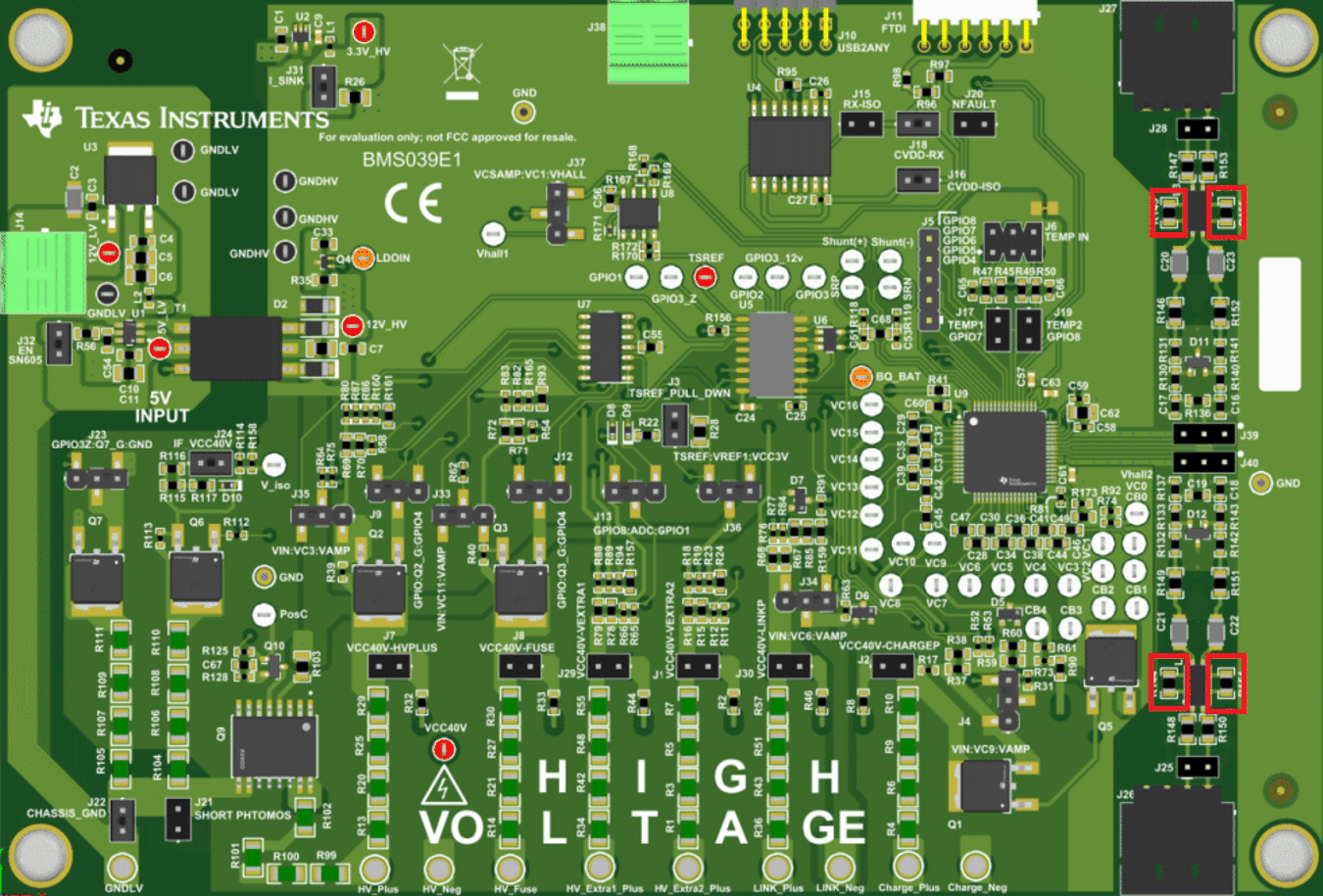
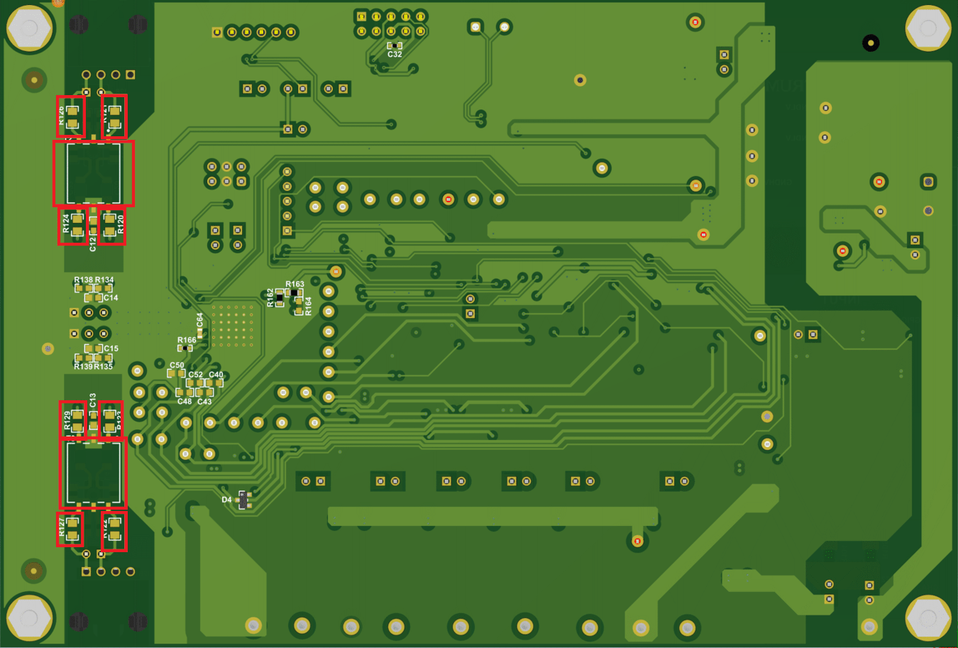
If the user wanted the daisy chain communications to be handled by the transformer, then de-solder the following resistors: R148, R149, R150, R151, R146, R147, R152, R153. On the underside of the EVM, populate the R122, R123, R127, R129, R120, R121, R124, and R126 slots with 0-Ω resistors and T2 and T3 with transformers. This allows the signal to flow through the underside of the EVM where the transformers (T2 and T3) are located.
 Figure 3-1 Resistors to De-solder
Topside
 Figure 3-2 Resistors to De-solder
Underside