SLDU028A January 2018 – March 2020 TPS65313-Q1
-
TPS65313-EVM User’s Guide
- Trademarks
- 1 TPS65313-EVM Top View With Basic External Connections
- 2 TPS65313-EVM Input, Output Voltages, and Load Current Requirements
- 3 TPS65313-EVM Jumper Settings
- 4 TPS65313-EVM GUI Installing and Opening the GUI
- 5 TPS65313-EVM Power-Up and Power-Down Procedure
- 6 TPS65313 GUI
- 7 TPS65313-EVM Typical Plots
- 8 TPS65313-EVM Schematic Diagram
- 9 TPS65313-EVM Part List
- 10 PCB Layer Diagram
- 11 Description of the Watchdog Algorithm Implemented on EVM
- Revision History
6.1.6 Enable Q&A Watchdog
To enable the device transition to the DIAGNOSTIC or ACTIVE state, the question and answer (Q&A) watchdog must be enabled and configured correctly. The device has two options for watchdog Q&A configurations: mode 0 and mode 1. The TPS65313-Q1 device exchanges questions and answers with the USB2ANY MCU within the timing specified in the timing fields on the GUI.
The default timing configurations are set when GUI is opened. When the device is in the SAFE state, enable the Enable Q&A Watchdog button to start the watchdog and sync it with MCU. When the watchdog is successfully synced, the WD fail counter starts to decrease and reaches 0.
When the watchdog is synced when the device is in the SAFE state, the SAFE to DIAGNOSTIC button can be clicked to make the device to go to the DIAGNOSTIC state. When the device is in the DIAGNOSTIC state, the DIAGNOSTIC to ACTIVE button can be clicked to put the device in the ACTIVE state.
If users want to try the different watchdog timing settings, adjust the watchdog timing settings only when the device is in the DIAGNOSTIC.
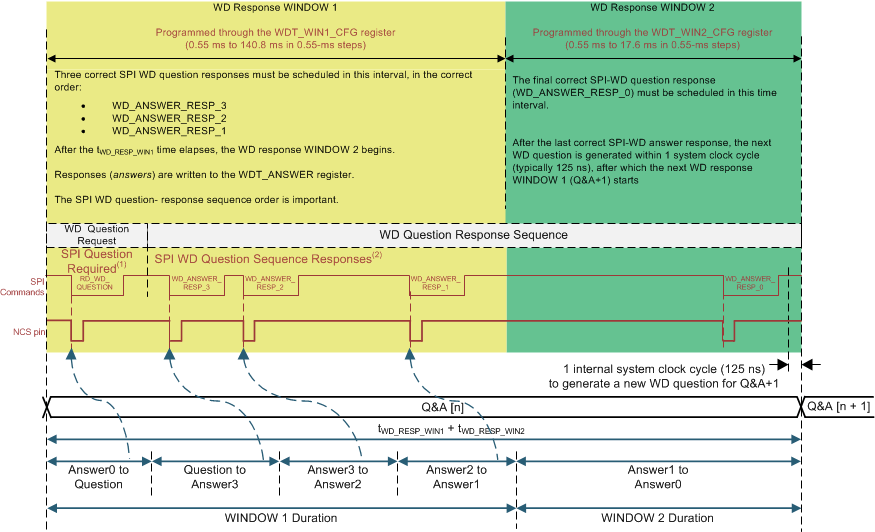
Figure 5 shows the timing diagram for the watchdog windows. Each setting or field in the GUI is defined as follows:
- Answer0 to Question (ms) This field is the time at which the WD question is received by the MCU (the GUI default is 30 ms).
- Question to Answer3 (ms) This field is the time at which Answer3 is sent from the MCU (the GUI default is 30 ms).
- Answer2 to Answer1 (ms) This field is the time at which Answer1 is sent from the MCU (the GUI default is 30 ms).
- Reset MCU Timings This button resets the MCU timing to the default GUI settings.
- Answer3 to Answer2 (ms) This field is the time at which Answer2 is sent from the MCU (the GUI default is 30 ms).
- Answer1 to Answer0 (ms) This field is the time at which Answer0 is sent from the MCU (the GUI default is 25 ms).
- Window1 Duration (ms) This field is the WD response WINDOW 1 duration set in the WDT_WIN1_CFG register (the GUI default is 140.8 ms).
- Window2 Duration (ms) This field is the WD response WINDOW 2 duration set in the WDT_WIN2_CFG register (the GUI default is 17.6 ms).
- Set Watchdog Settings Whenever the watchdog timing is changed, click this button to update the WD_WIN1_CFG and WD_WIN2_CFG registers with the set timing values and to also sync the MCU timings again.
- Read Window Durations Click this button to read back the values of the WD_WIN1_CFG and WD_WIN2_CFG registers and update the timing values in the Window1 Duration (ms) and Window2 Duration (ms) fields.
 Figure 5. Watchdog Window Timing Diagram
 Section 11 describes the watchdog implementation on the MSP430™ MCU on the EVM.