SLAU298A November 2009 – May 2021
- Trademarks
- 1ADS8555EVM-PDK Overview
- 2EVM Analog Interface
- 3Digital Interface
- 4Power Supplies
- 5Installing the ADS8555EVM Software
-
6ADS8555EVM Operation
- 6.1 Connecting the Hardware and Running the GUI
- 6.2 Jumper Settings for the ADS8555EVM
- 6.3 Modifying Hardware and Using Software to Evaluate Other Devices in the Family
- 6.4 EVM GUI Global Settings for ADC Control and Registers
- 6.5 Time Domain Display
- 6.6 Frequency Domain Display
- 6.7 Histogram Display
- 7Bill of Materials, Layout, and Schematics
- 8Revision History
3.4 Connections to the PHI Connector
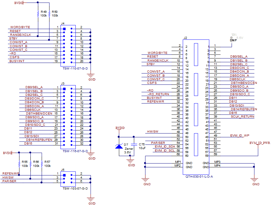
Connector J2 is used to connect the PHI digital controller printed circuit board (PCB) to the ADS8555EVM. This connector has all the digital signals as well as the BVDD supply. The power for the BVDD supply is from the USB connection. This connector also provides I2C signals that are used on the EEPROM identification circuit. The digital signals can be monitored on the J3, J4, and J5 test headers. Figure 3-2 provides a schematic showing the various connections to the PHI connector.
 Figure 3-2 Connections to PHI
Connector