SLAU298A November 2009 – May 2021
- Trademarks
- 1ADS8555EVM-PDK Overview
- 2EVM Analog Interface
- 3Digital Interface
- 4Power Supplies
- 5Installing the ADS8555EVM Software
-
6ADS8555EVM Operation
- 6.1 Connecting the Hardware and Running the GUI
- 6.2 Jumper Settings for the ADS8555EVM
- 6.3 Modifying Hardware and Using Software to Evaluate Other Devices in the Family
- 6.4 EVM GUI Global Settings for ADC Control and Registers
- 6.5 Time Domain Display
- 6.6 Frequency Domain Display
- 6.7 Histogram Display
- 7Bill of Materials, Layout, and Schematics
- 8Revision History
2.1 ADC Supply, Input, Voltage Reference, and Digital Connections
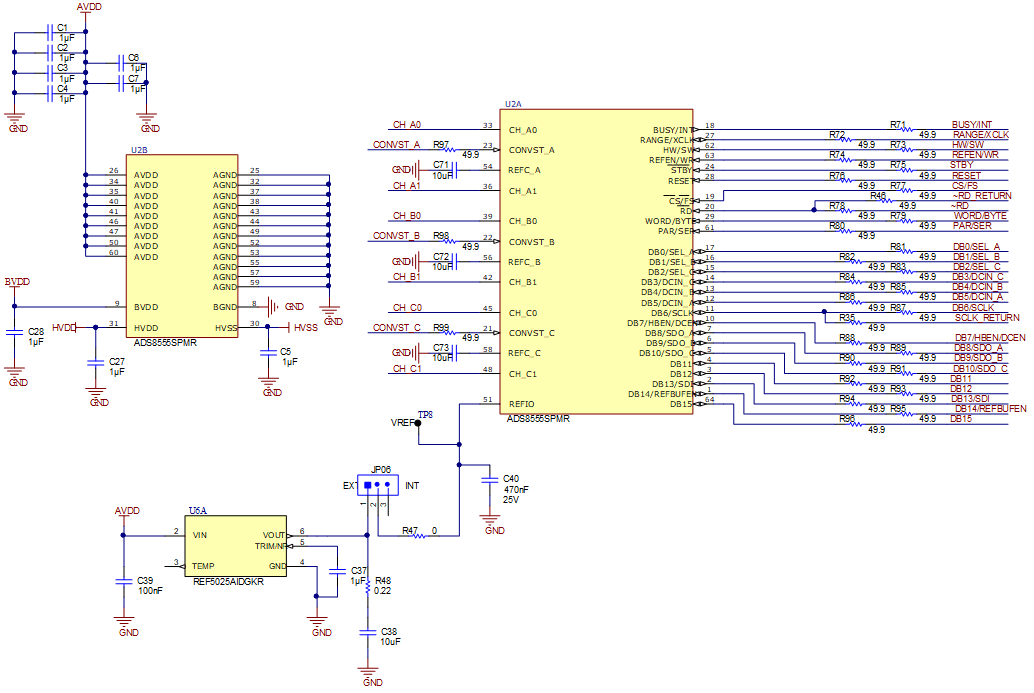
Figure 2-1 shows the decoupling on AVDD, BVDD, HVDD, and HVSS and the voltage reference. The decoupling capacitors match the recommendations in the ADS8555 data sheet. The layout (see Figure 7-1) uses the shortest possible connections to the decoupling capacitors and connects the ground end to the GND plane using vias. The ADS8555 can use an external or internal voltage reference. This reference can be selected by changing the position of JP06 to INT for internal or EXT for external. Figure 2-1 also shows the analog input signal and digital signal connections.
 Figure 2-1 ADC Signal and Supply Connection