SLAU298A November 2009 – May 2021
- Trademarks
- 1ADS8555EVM-PDK Overview
- 2EVM Analog Interface
- 3Digital Interface
- 4Power Supplies
- 5Installing the ADS8555EVM Software
-
6ADS8555EVM Operation
- 6.1 Connecting the Hardware and Running the GUI
- 6.2 Jumper Settings for the ADS8555EVM
- 6.3 Modifying Hardware and Using Software to Evaluate Other Devices in the Family
- 6.4 EVM GUI Global Settings for ADC Control and Registers
- 6.5 Time Domain Display
- 6.6 Frequency Domain Display
- 6.7 Histogram Display
- 7Bill of Materials, Layout, and Schematics
- 8Revision History
4.1 External Power Connections and Test Points
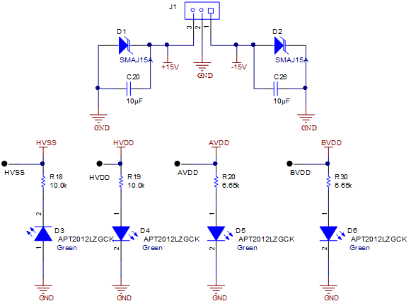
The screw terminal block J1 is used to connect the external high voltage supplies. These supplies are not provided in the evaluation module kit and the expectation is that a low-noise lab supply is used to provide this power (for example, Keysight™ E3632A). The high-voltage supplies have transient voltage suppressor diodes to help protect the ADC from transients. These supplies are typically connected to ±15 V. For details on operation, see the ADS8555 data sheet. Figure 4-1 also shows how each supply has a light-emitting diode (LED) monitor for quick verification that power is applied.
 Figure 4-1 External Power Connections and
Test Points