SLAA721E October   2016  – March 2020 MSP430FR5969 , MSP430FR5969-SP , MSP430FR5994 , MSP430FR6989


  1.   Trademarks
  2. 1Introduction
    1. 1.1 Glossary
    2. 1.2 Conventions
  3. 2Implementation
    1. 2.1 Main
    2. 2.2 Application Manager
      1. 2.2.1 Bootloader and Application Detection
        1. 2.2.1.1 Forcing Bootloader Mode
        2. 2.2.1.2 Application Validation
        3. 2.2.1.3 Jumping to Application
      2. 2.2.2 Memory Assignment
      3. 2.2.3 Interrupt Vectors in FRAM Devices
    3. 2.3 Memory Interface (MI)
      1. 2.3.1 Dual Image Support
    4. 2.4 Communication Interface (CI)
      1. 2.4.1 Physical-DataLink (PHY-DL)
        1. 2.4.1.1 UART
        2. 2.4.1.2 SPI
        3. 2.4.1.3 CC110x
        4. 2.4.1.4 Comm Sharing
      2. 2.4.2 NWK-APP
        1. 2.4.2.1 BSL-Based Protocol
          1. 2.4.2.1.1 Security
          2. 2.4.2.1.2 BSL-Based Protocol Using CC110x
          3. 2.4.2.1.3 Examples Using UART or CC110x
  4. 3Customization of MSP430FRBoot
    1. 3.1 Predefined Customizations
  5. 4Building MSPBoot
    1. 4.1 LaunchPad™ Development Kit Hardware
    2. 4.2 CC110x Hardware
    3. 4.3 Software
      1. 4.3.1 Building the Target Software
      2. 4.3.2 Convert Application Output Images
      3. 4.3.3 Generating Linker Files
  6. 5Demo Using FRAM LaunchPad Development Kit as Host
    1. 5.1 Hardware
    2. 5.2 Building the Host Project
    3. 5.3 Running the Demo
  7. 6Porting the target side example projects to other MSP430FR devices
  8. 7References
  9. 8Revision History

SPI

The SPI interface, used for CC110x communication, is implemented using the following configuration (also see Figure 2-7):

  • 8-bit data
  • MSB first
  • Clock polarity = 0 (inactive state is low)
  • Clock phase = 1 (data captured on first clock edge, changed on following edge)
  • 3-pin configuration with STE implemented using GPIO
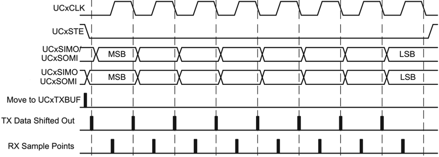
GUID-857F6F1E-1DB5-4C7B-8E9D-3BBB7893E3AC-low.pngFigure 2-7 SPI Format