SLUS652E March 2005 – April 2020 UCD8220
PRODUCTION DATA.
- 1 Features
- 2 Applications
- 3 Description
- 4 Revision History
- 5 Pin Configuration and Functions
- 6 Specifications
- 7 Detailed Description
- 8 Application and Implementation
- 9 Power Supply Recommendations
- 10Layout
- 11Device and Documentation Support
- 12Mechanical, Packaging, and Orderable Information
封装选项
请参考 PDF 数据表获取器件具体的封装图。
机械数据 (封装 | 引脚)
- PWP|16
散热焊盘机械数据 (封装 | 引脚)
- PWP|16
订购信息
6.7 Typical Characteristics
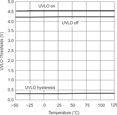 Figure 2. UCD8220 UVLO Threshold vs Temperature
 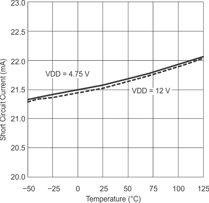 Figure 4. 3V3 Short-circuit Current vs Temperature
 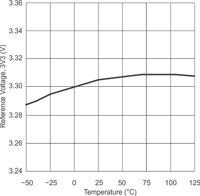 Figure 3. 3V3 Reference Voltage vs Temperature
 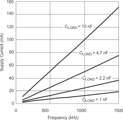 Figure 5. Supply Current vs Frequency (VDD = 5 V)
 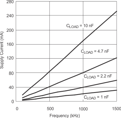 Figure 6. Supply Current vs Frequency (VDD = 8 V)
 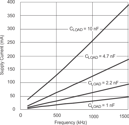 Figure 8. Supply Current vs Frequency (VDD = 12 V)
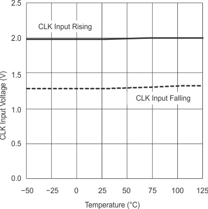
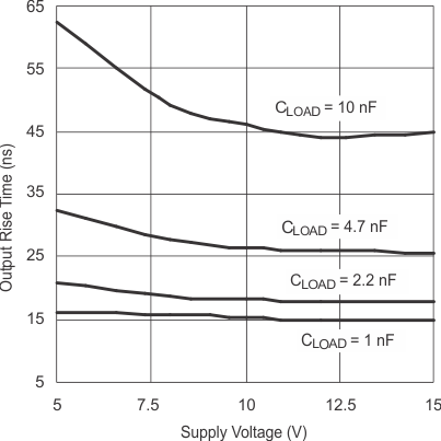
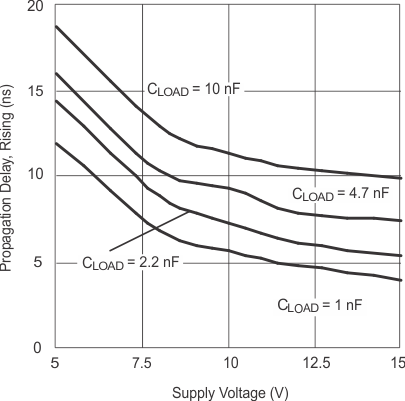 Figure 14. CLK to OUTx Propagation Delay Rising vs Supply Voltage
 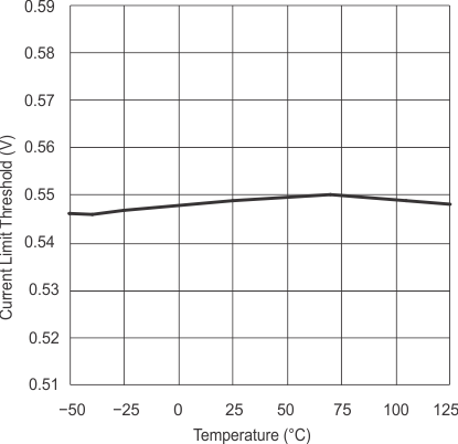 Figure 16. Default Current Limit Threshold vs Temperature
 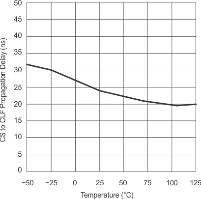 Figure 18. CS to CLF Propagation Delay vs Temperature
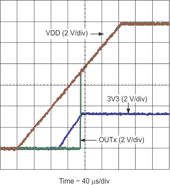
| CLK = CTRL = 3V3 |
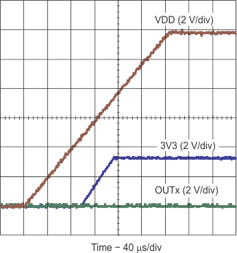
| CLK = AGND | CTRL = 3V3 |
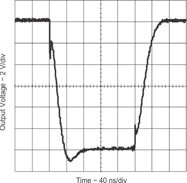
| VDD = 12 V | CLOAD = 10 nF |
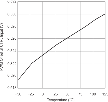
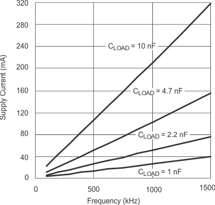 Figure 7. Supply Current vs Frequency (VDD = 10 V)
 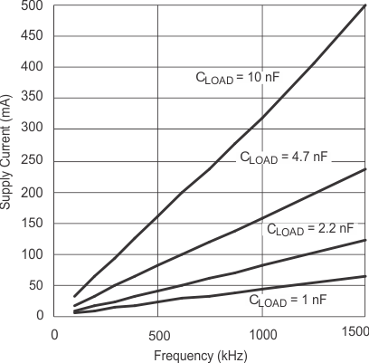 Figure 9. Supply Current vs Frequency (VDD = 15 V)
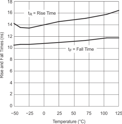
| CLOAD = 2.2 nF | VDD = 12 V |
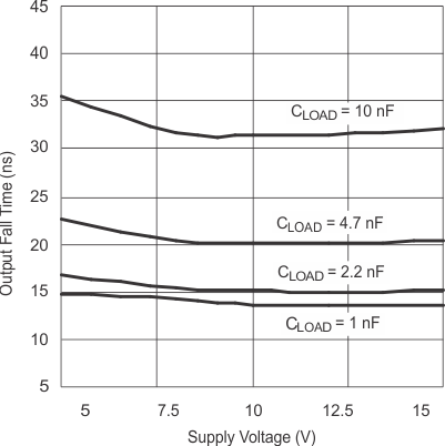
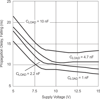 Figure 15. CLK to OUTx Propagation Delay Falling vs Supply Current
 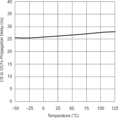 Figure 17. CS to OUTx Propagation Delay vs Temperature
 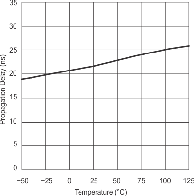 Figure 19. CLK to OUT Propagation Delay vs Temperature
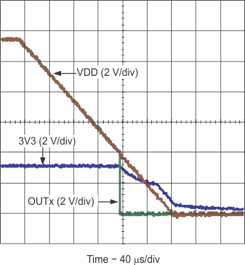
| CLK = CTRL = 3V3 |
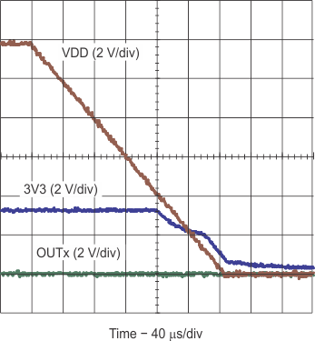
| CLK = AGND | CTRL = 3V3 |
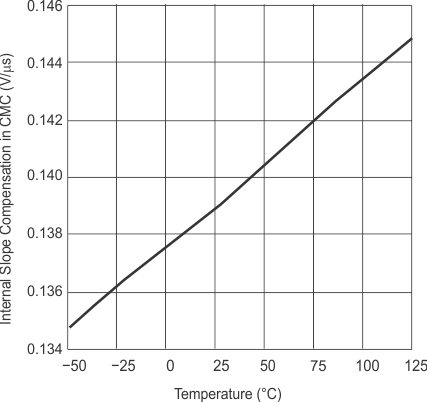
| Current mode slope | RISET = 100 kΩ |