SLUS652E March 2005 – April 2020 UCD8220
PRODUCTION DATA.
- 1 Features
- 2 Applications
- 3 Description
- 4 Revision History
- 5 Pin Configuration and Functions
- 6 Specifications
- 7 Detailed Description
- 8 Application and Implementation
- 9 Power Supply Recommendations
- 10Layout
- 11Device and Documentation Support
- 12Mechanical, Packaging, and Orderable Information
封装选项
请参考 PDF 数据表获取器件具体的封装图。
机械数据 (封装 | 引脚)
- PWP|16
散热焊盘机械数据 (封装 | 引脚)
- PWP|16
订购信息
6.6 Timing Requirements
VDD = 12 V, 4.7-µF capacitor from VDD to AGND, 1 μF from PVDD to PGND, 0.22-µF capacitor from 3V3 to AGND, TA = TJ = –40°C to 105°C, (unless otherwise noted).| MIN | NOM | MAX | UNIT | |||
|---|---|---|---|---|---|---|
| CLOCK INPUT (CLK) | ||||||
| Minimum allowable off time(1) | 20 | ns | ||||
| CURRENT LIMIT (ILIM) | ||||||
| Propagation delay from CLK to CLF | CLK rising to CLF falling after a current limit event | 15 | 25 | ns | ||
| CURRENT SENSE COMPARATOR | ||||||
| Propagation delay from CS to OUTx | ILIM = 0.5 V, measured on OUTx, CS = threshold + 60 mV | 25 | 40 | ns | ||
| Propagation delay from CS to CLF | ILIM = 0.5 V, measured on CLF, CS = threshold + 60 mV | 25 | 50 | |||
| OUTPUT DRIVERS | ||||||
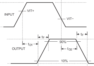
| tR | Rise time | CLOAD = 2.2 nF, VDD = 12 V, See Figure 1 | 10 | 20 | ns | |
| tF | Fall time | CLOAD = 2.2 nF, VDD = 12 V, See Figure 1 | 10 | 15 | ||
| tD1 | Propagation delay from CLK to OUTx, CLK rising | CLOAD = open, VDD = 12 V, See Figure 1 | 25 | 35 | ns | |
| tD2 | Propagation delay from CLK to OUTx, CLK falling | CLOAD = open, VDD = 12 V, See Figure 1 | 25 | 35 | ||
 Figure 1. Timing Diagram