SLUS652E March 2005 – April 2020 UCD8220
PRODUCTION DATA.
- 1 Features
- 2 Applications
- 3 Description
- 4 Revision History
- 5 Pin Configuration and Functions
- 6 Specifications
- 7 Detailed Description
- 8 Application and Implementation
- 9 Power Supply Recommendations
- 10Layout
- 11Device and Documentation Support
- 12Mechanical, Packaging, and Orderable Information
封装选项
请参考 PDF 数据表获取器件具体的封装图。
机械数据 (封装 | 引脚)
- PWP|16
散热焊盘机械数据 (封装 | 引脚)
- PWP|16
订购信息
8.2.2.1 Selecting the ISET Resistor for Voltage Mode Control
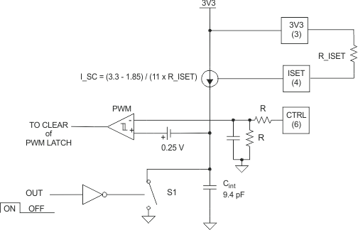
 Figure 31. UCD8220 Configured in Voltage Mode Control With an Internal Timing Capacitor
 When the ISET resistor is configured as shown in Figure 31 with the ISET resistor connected between the ISET pin and the 3V3 pin, the device is set up for voltage mode control. For purposes of voltage loop compensation the, voltage ramp is 1.4 V from the valley to the peak. Use Equation 5 to calculate the proper resistance for a desired clock frequency.

where
- fclk = desired clock frequency in Hz
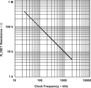
 Figure 32. ISET Resistance Versus Clock Frequency
 Figure 32 shows the nominal value of resistance to use for a desired clock frequency. For example, a clock frequency of 1000 kHz will require 10 kΩ of the ISET resistor. The UCD8220 device has two outputs controlled by push-pull logic and therefore the output ripple frequency is equal to the clock frequency and each output switches at half the clock frequency.