SLUS652E March   2005  – April 2020 UCD8220

PRODUCTION DATA.  

  1. Features
  2. Applications
  3. Description
    1. 3.1 UCD8220 Typical Simplified Push-Pull Converter Application Schematic
  4. Revision History
  5. Pin Configuration and Functions
    1.     Pin Functions
  6. Specifications
    1. 6.1 Absolute Maximum Ratings
    2. 6.2 ESD Ratings
    3. 6.3 Recommended Operating Conditions
    4. 6.4 Thermal Information
    5. 6.5 Electrical Characteristics
    6. 6.6 Timing Requirements
    7. 6.7 Typical Characteristics
  7. Detailed Description
    1. 7.1 Overview
    2. 7.2 Functional Block Diagram
    3. 7.3 Feature Description
      1. 7.3.1 CLK Input Time-Domain Digital Pulse Train
      2. 7.3.2 Current Sensing and Protection
      3. 7.3.3 Handshaking
      4. 7.3.4 Driver Output
      5. 7.3.5 Source and Sink Capabilities During Miller Plateau
      6. 7.3.6 Drive Current and Power Requirements
      7. 7.3.7 Clearing the Current-Limit Flag (CLF)
    4. 7.4 Device Functional Modes
  8. Application and Implementation
    1. 8.1 Application Information
    2. 8.2 Typical Application
      1. 8.2.1 Design Requirements
      2. 8.2.2 Detailed Design Procedure
        1. 8.2.2.1 Selecting the ISET Resistor for Voltage Mode Control
        2. 8.2.2.2 Selecting the ISET Resistor for Voltage Mode Control with Voltage Feed Forward
        3. 8.2.2.3 Selecting the ISET Resistor for Peak Current Mode Control with Internal Slope Compensation
      3. 8.2.3 Application Curves
  9. Power Supply Recommendations
  10. 10Layout
    1. 10.1 Layout Guidelines
    2. 10.2 Layout Example
    3. 10.3 Thermal Considerations
  11. 11Device and Documentation Support
    1. 11.1 Documentation Support
      1. 11.1.1 Related Documentation
    2. 11.2 Trademarks
    3. 11.3 Electrostatic Discharge Caution
    4. 11.4 Glossary
  12. 12Mechanical, Packaging, and Orderable Information

封装选项

请参考 PDF 数据表获取器件具体的封装图。

机械数据 (封装 | 引脚)
  • PWP|16
散热焊盘机械数据 (封装 | 引脚)
订购信息

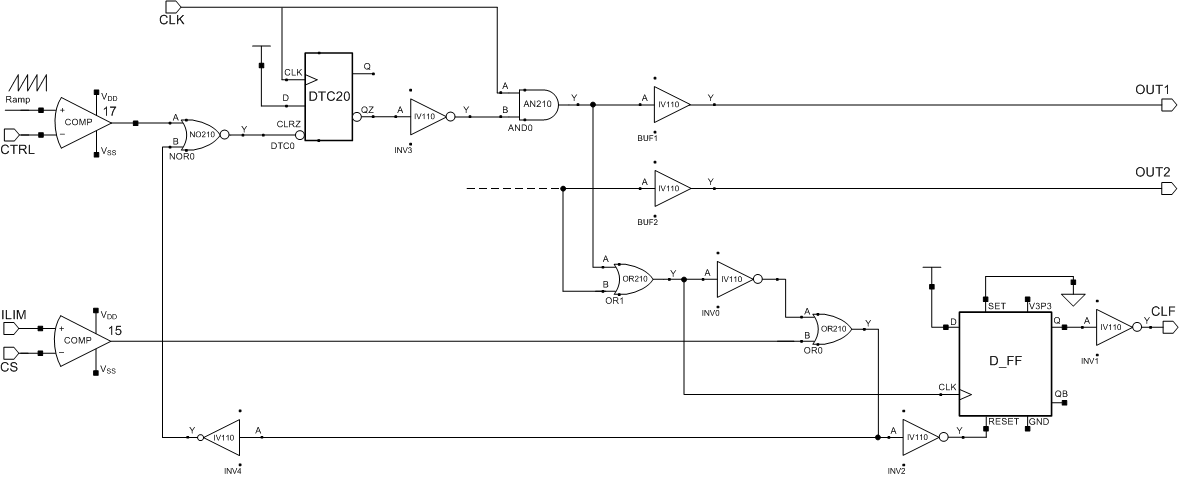
Clearing the Current-Limit Flag (CLF)

In the UCD8220 design, the CLF signal is cleared by the comparator (compares the voltage between the CS and ILIM pins) output. However, the comparator output is enabled by the OUTx pin. Therefore, the CLF signal does not clear (go low) unless one or both OUTx pins are on, which enables the comparator output. Pulling the CTRL pin high turns the OUTx pin on which is why the CLF flag only clears when CTRL is high (greater than 0.45 to 0.6 V). Therefore, anything that turns on the OUTs pins enables the comparator, and if V_CS is less than V_ILIM, the comparator output clears the CLF signal. The CLF signal goes low during the next rising edge on the CLK pin after these conditions are met.
UCD8220 dd_cfl_slusb36.gifFigure 29. Logic Circuit for CLF