ZHCSR36A December 2022 – October 2025 TPS748A
PRODUCTION DATA
7.4.1 布局指南
适当的布局可以极大地改善瞬态性能、PSRR 和噪声。为更大程度地减小负载瞬态期间器件输入端的压降,将 IN 和 BIAS 上的电容连接至尽可能靠近器件的位置。该电容还可以更大限度减小寄生电感和输入源电阻的影响,从而提高稳定性。为实现最佳的瞬态性能和精度,将 图 7-1 中 R1 的顶侧尽可能靠近负载连接。如果 BIAS 连接到 IN,则将 BIAS 连接到尽可能靠近输入电源的检测点的位置。该连接可在瞬态条件下更大限度地减少 BIAS 上的压降,并可以改善导通响应。
了解器件功率耗散并正确确定连接到散热焊盘的热平面尺寸至关重要。这些参数有助于避免器件出现热关断,确保其稳定运行。器件的功率耗散可通过 方程式 11 计算得出,并取决于输入电压和负载条件。
方程式 11. 
通过使用实现所需输出电压的最低可能输入电压,大大减小功率耗散并提高效率。
在 VSON (DRC) 封装上,主要的热传导路径是通过外露焊盘到达印刷电路板 (PCB)。将此焊盘接地或保持悬空。但是,需确认散热焊盘已连接到适当大小的铜 PCB 区域,以防止器件过热。最大结温至环境温度热阻可以使用方程式 12 计算,取决于最高环境温度、最高器件结温和器件的功率耗散。
方程式 12. 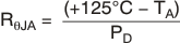
适当散热所需最小 PCB 铜面积使用(使用 图 7-3 估算),由已知的最大 RθJA 来确定。

电路板尺寸为 9in2(即 3in × 3in)时的 RθJA 值是 JEDEC 标准。
图 7-3 RθJA 与电路板尺寸之间的关系图 7-3 展示了 RθJA 与电路板中接地平面覆铜区的函数关系。此图仅作为展示接地平面中散热效果的参考指南。此图不能用于估算实际应用环境中的实际热性能。
注: 器件安装在应用 PCB 上时,使用 ΨJT 和 ΨJB,参见估算结温部分中的说明。