ZHCSM62C September   2020  – December 2021 TPS542A50

PRODUCTION DATA  

  1. 特性
  2. 应用
  3. 说明
  4. Revision History
  5. Pin Configuration and Functions
  6. Specifications
    1. 6.1 Absolute Maximum Ratings
    2. 6.2 ESD Ratings
    3. 6.3 Recommended Operating Conditions
    4. 6.4 Thermal Information
    5. 6.5 Electrical Characteristics
    6. 6.6 Typical Characteristics
  7. Detailed Description
    1. 7.1 Overview
    2. 7.2 Functional Block Diagram
    3. 7.3 Feature Description
      1. 7.3.1  Enable and Adjustable Undervoltage Lockout
      2. 7.3.2  Input and VREG Undervoltage Lockout Protection
      3. 7.3.3  Voltage Reference and Setting the Output Voltage
      4. 7.3.4  Remote Sense Function
      5. 7.3.5  Switching Frequency
      6. 7.3.6  Voltage Control Mode Internal Compensation
      7. 7.3.7  Soft Start and Prebiased Output Start-up
      8. 7.3.8  Power Good
      9. 7.3.9  Overvoltage and Undervoltage Protection
      10. 7.3.10 Overcurrent Protection
      11. 7.3.11 High-Side FET Throttling
      12. 7.3.12 Overtemperature Protection
    4. 7.4 Device Functional Modes
      1. 7.4.1 Pulse-Frequency Modulation Eco-mode Light Load Operation
      2. 7.4.2 Forced Continuous-Conduction Mode
      3. 7.4.3 Soft Start
    5. 7.5 Programming
      1. 7.5.1 I2C Address Selection
      2. 7.5.2 Powering Device Into Programming Mode
      3. 7.5.3 Device Configuration
      4. 7.5.4 Output Voltage Adjustment
    6. 7.6 Pin-Strap Programming
    7. 7.7 Register Maps
      1. 7.7.1 ID Register (Offset = 0x0) [reset = 0x21]
      2. 7.7.2 STATUS Register (Offset = 0x1) [reset = 0x0]
      3. 7.7.3 VOUT_ADJ1 Register (Offset = 0x2) [reset = 0x0]
      4. 7.7.4 VOUT_ADJ2 Register (Offset = 0x3) [reset = 0x0]
      5. 7.7.5 CONFIG1 Register (Offset = 0x4) [reset = 0x0B]
      6. 7.7.6 CONFIG2 Register (Offset = 0x5) [reset = 0x2D]
  8. Application and Implementation
    1. 8.1 Application Information
    2. 8.2 Typical Application
      1. 8.2.1 Full Analog Configuration
        1. 8.2.1.1 Design Requirements
        2. 8.2.1.2 Detailed Design Procedure
          1. 8.2.1.2.1  Custom Design With WEBENCH® Tools
          2. 8.2.1.2.2  Output Voltage Calculation
          3. 8.2.1.2.3  Switching Frequency Selection
          4. 8.2.1.2.4  Inductor Selection
          5. 8.2.1.2.5  Input Capacitor Selection
          6. 8.2.1.2.6  Bootstrap Capacitor Selection
          7. 8.2.1.2.7  R-C Snubber and VIN Pin High-Frequency Bypass
          8. 8.2.1.2.8  Output Capacitor Selection
          9. 8.2.1.2.9  Response to a Load Transient
          10. 8.2.1.2.10 Pin-Strap Setting
        3. 8.2.1.3 Application Curves
        4. 8.2.1.4 Typical Application Circuits
  9. Power Supply Recommendations
  10. 10Layout
    1. 10.1 Layout Guidelines
    2. 10.2 Layout Example
  11. 11Device and Documentation Support
    1. 11.1 Device Support
      1. 11.1.1 Development Support
        1. 11.1.1.1 Fusion Digital Power™ Designer Tool
        2. 11.1.1.2 Custom Design With WEBENCH® Tools
    2. 11.2 接收文档更新通知
    3. 11.3 支持资源
    4. 11.4 Trademarks
    5. 11.5 Electrostatic Discharge Caution
    6. 11.6 术语表
  12. 12Mechanical, Packaging, and Orderable Information

封装选项

机械数据 (封装 | 引脚)
散热焊盘机械数据 (封装 | 引脚)
订购信息

Typical Characteristics

Measured at 25°C unless otherwise specified
Measured at 25°C unless otherwise specifiedGUID-C1DB4A39-B434-4E7E-869B-47C5175D75E5-low.gif
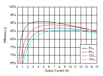
VOUT = 1 V fSW = 1 MHz, FCCM
Figure 6-1 Efficiency vs Output Current. Measured at 25°C unless otherwise specified
GUID-684EE346-BC01-4C5D-822D-9689E6118CCE-low.gif
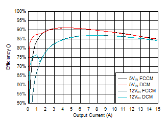
VOUT = 1 V fSW = 1 MHz, DCM versus FCCM
Figure 6-3 Efficiency vs Output Current
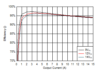
GUID-A758A838-F449-41B5-943C-B13CA73DA020-low.gif
VOUT = 5 V fSW = 400 kHz, FCCM
Figure 6-5 Efficiency vs Output Current
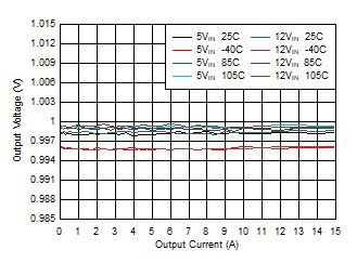
GUID-EB15B3C7-7A48-4F5B-8136-C0C8FFAE2D4F-low.gif
VOUT = 1 V fSW = 1 MHz, FCCM
Figure 6-7 Load Regulation
GUID-85BF5A50-B284-40F3-8347-FA40777B4D12-low.gif
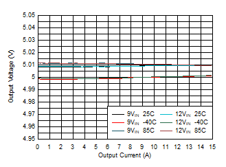
VIN = 12 VVOUT = 5 VfSW = 400 KHz, FCCM
Figure 6-9 Load Regulation
GUID-7DB5293F-A5B1-4695-9D67-EE44A4FFE3AA-low.gif
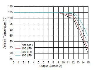
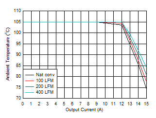
VIN = 12 VVOUT = 5 VfSW = 600 kHz
Figure 6-11 Ambient Temperature vs Output Current
GUID-7AA6CD31-C986-4681-A4DA-9EF574D957DC-low.gif
VIN = 12 V VOUT = 1 V fSW = 1 MHz
Figure 6-13 Thermal Image at 15-A Output Current
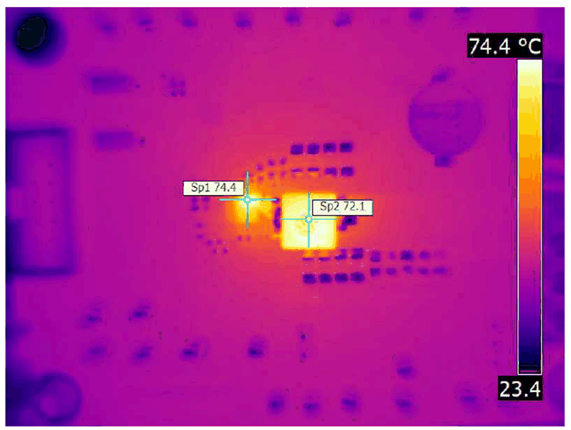
GUID-BF0C8756-01AE-4B15-AB0E-507C29318552-low.gif
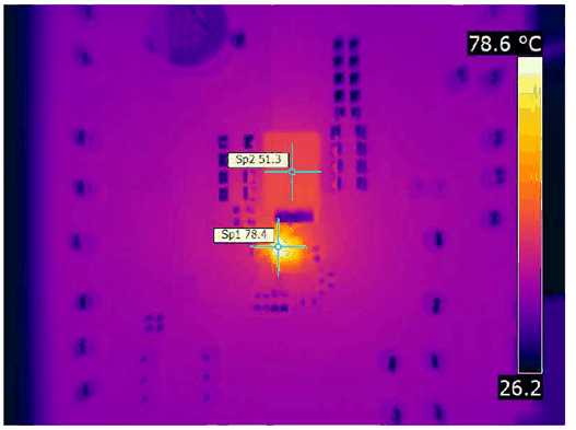
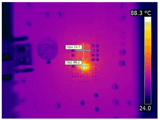
VIN = 12 V VOUT = 5 V fSW = 0.6 MHz
Figure 6-15 Thermal Image at 12-A Output Current
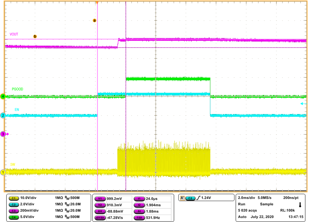
GUID-20200811-CA0I-4HFG-FWPT-RL20RKQXBWTP-low.png
VIN = 12 V VOUT = 1 V fSW = 1.0 MHz BOM
Figure 6-17 90% Pre-biased Start-up by EN at 0-A Output Current
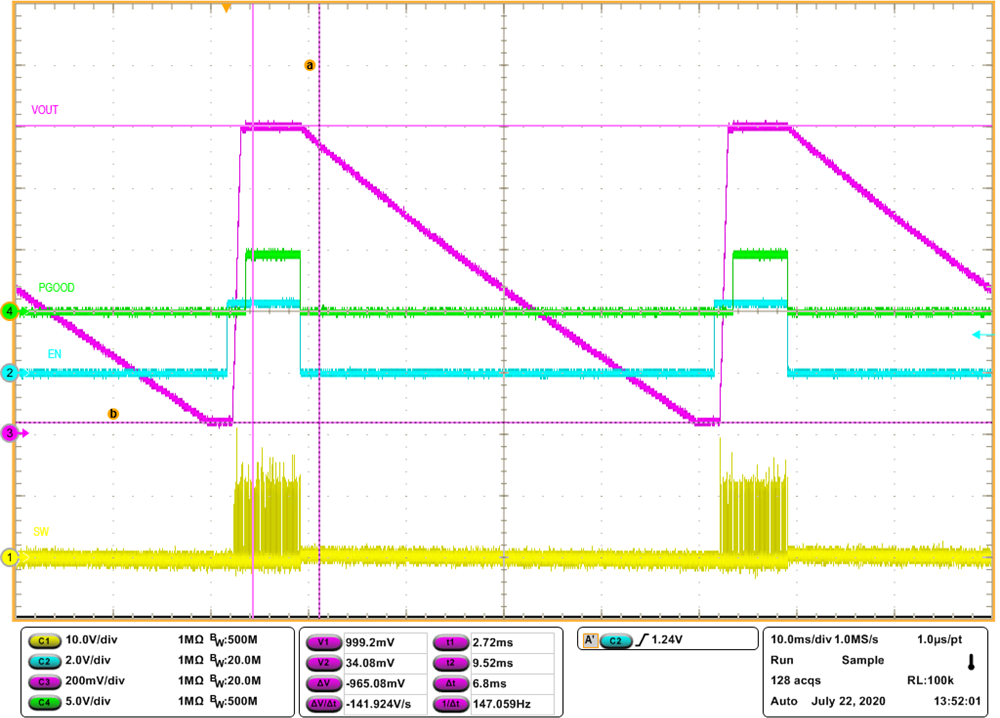
GUID-20200811-CA0I-DXR9-WSCM-VL9L7DFNMLVH-low.png
VIN = 12 V VOUT = 1 V fSW = 1.0 MHz BOM
Figure 6-19 Start-up and Shutdown by EN at 0-A Output Current
GUID-20200811-CA0I-CT31-Z424-GCKLGLGD4TWR-low.png
VIN = 12 V VOUT = 1 V fSW = 1.0 MHz BOM
Figure 6-21 Steady State at 10-A Output Current
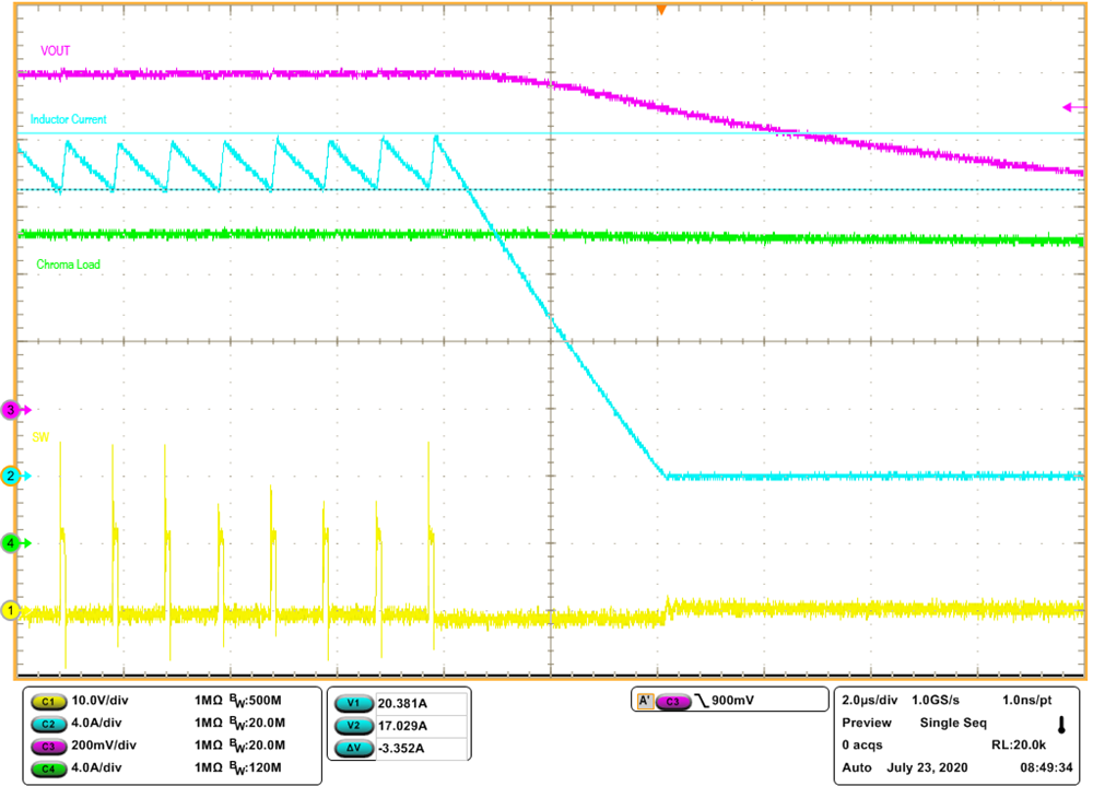
GUID-20200811-CA0I-W2SR-BJGJ-QKVPSZ5KC3TF-low.png
VIN = 12 V VOUT = 1 V fSW = 1.0 MHz BOM
Figure 6-23 20-A Overcurrent Protection by Electronic Load
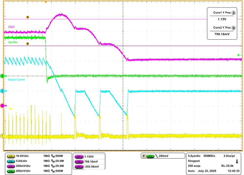
GUID-20200811-CA0I-FX6T-WV3B-HTT1DTZXKDTH-low.png
VIN = 12 V VOUT = 1 V fSW = 1.2 MHz BOM
Figure 6-25 Overvoltage Protection, Negative OCP, then Undervoltage Protection by Load Stepdown
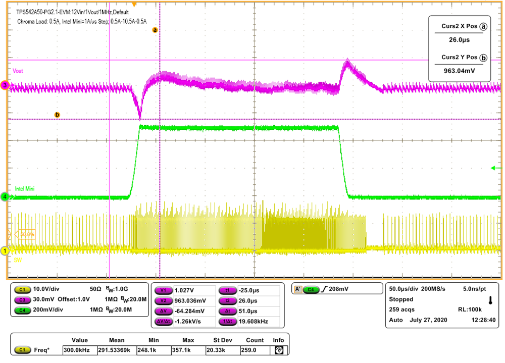
GUID-20200811-CA0I-M6KJ-HBZH-QC7HPJ5M1NM3-low.png
VIN = 12 V VOUT = 1 V fSW = 1.0 MHz BOM
Figure 6-27 Load Transient in DCM to FCM 0.5 A to 10.5 A to 0.5 A at 1 A/μs
GUID-765836A7-AA7E-461B-888E-6ECED9704CA6-low.gif
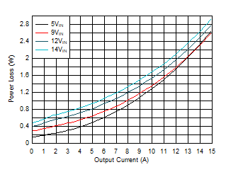
VOUT = 1 V fSW = 1 MHz, FCCM
Figure 6-2 Power Loss vs Output Current
GUID-5951D2C0-6C33-470C-AC24-D6446F8C068C-low.gif
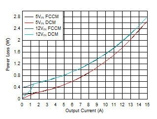
VOUT = 1 V fSW = 1 MHz, DCM versus FCCM
Figure 6-4 Power Loss vs Output Current
GUID-91CFDA1D-F75E-47D0-9D81-69C9724AC247-low.gif
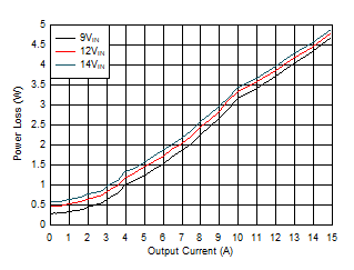
VOUT = 5 V fSW = 400 kHz, FCCM
Figure 6-6 Power Loss vs Output Current
GUID-B32A140F-20C1-4A8E-A700-A8CC7C6CEDA4-low.gif
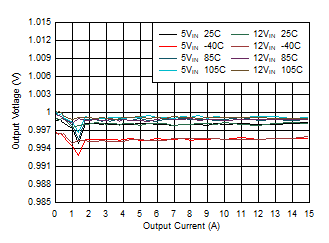
VOUT = 1 V fSW = 1 MHz, DCM
Figure 6-8 Load Regulation
GUID-DBD622FF-0ADE-4133-923F-720A9C2D3EDF-low.gif
VIN = 12 VVOUT = 1 VfSW = 1 MHz
Figure 6-10 Ambient Temperature vs Output Current
GUID-486DB8E3-38B9-4FA2-9196-43F5745B73AF-low.gif
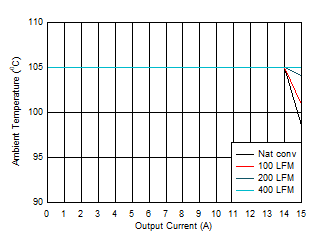
VIN = 5.5 VVOUT = 1 VfSW = 2.2 MHz
Figure 6-12 Ambient Temperature vs Output Current
GUID-696BA130-0320-430A-B29F-8D15DC4A6D58-low.gif
VIN = 5.5 V VOUT = 1 V fSW = 2.2 MHz
Figure 6-14 Thermal Image at 14-A Output Current
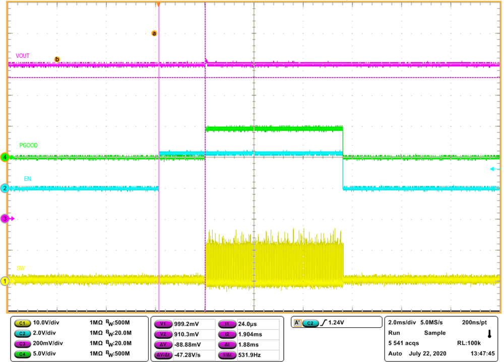
GUID-20200811-CA0I-NHMM-K5XT-1NVTF3W8XGRS-low.png
VIN = 12 V VOUT = 1 V fSW = 1.0 MHz BOM
Figure 6-16 100% Pre-biased Start-up by EN at 0-A Output Current
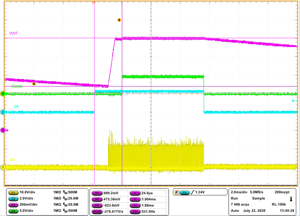
GUID-20200811-CA0I-15W3-SCV5-9L7TQQS6X5VJ-low.png
VIN = 12 V VOUT = 1 V fSW = 1.0 MHz BOM
Figure 6-18 50% Pre-biased Start-up by EN at 0-A Output Current
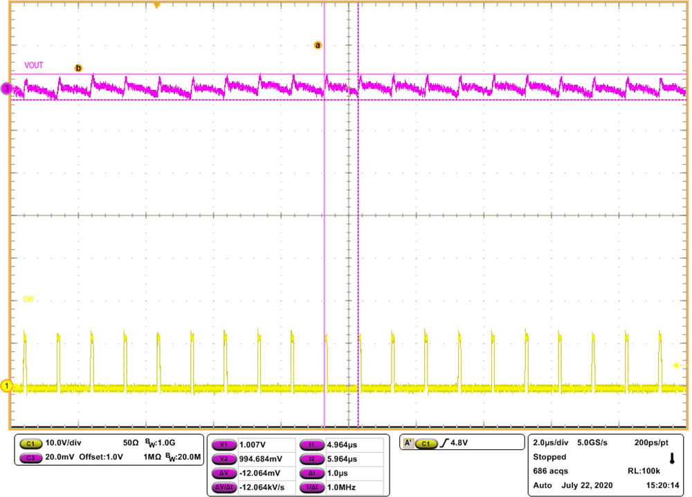
GUID-20200811-CA0I-96T7-KQRW-CGMMLL0PJ9TM-low.png
VIN = 12 V VOUT = 1 V fSW = 1.0 MHz BOM
Figure 6-20 Steady State at 0-A Output Current
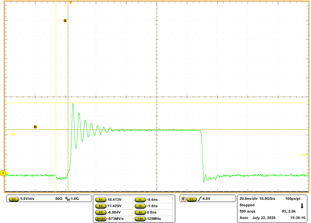
GUID-20200811-CA0I-XJLB-0VJS-XBLPQRMFKLV8-low.png
VIN = 12 V VOUT = 1 V fSW = 1.0 MHz BOM
Figure 6-22 Switch Node Ringing and Dead-Time at 10-A Output Current
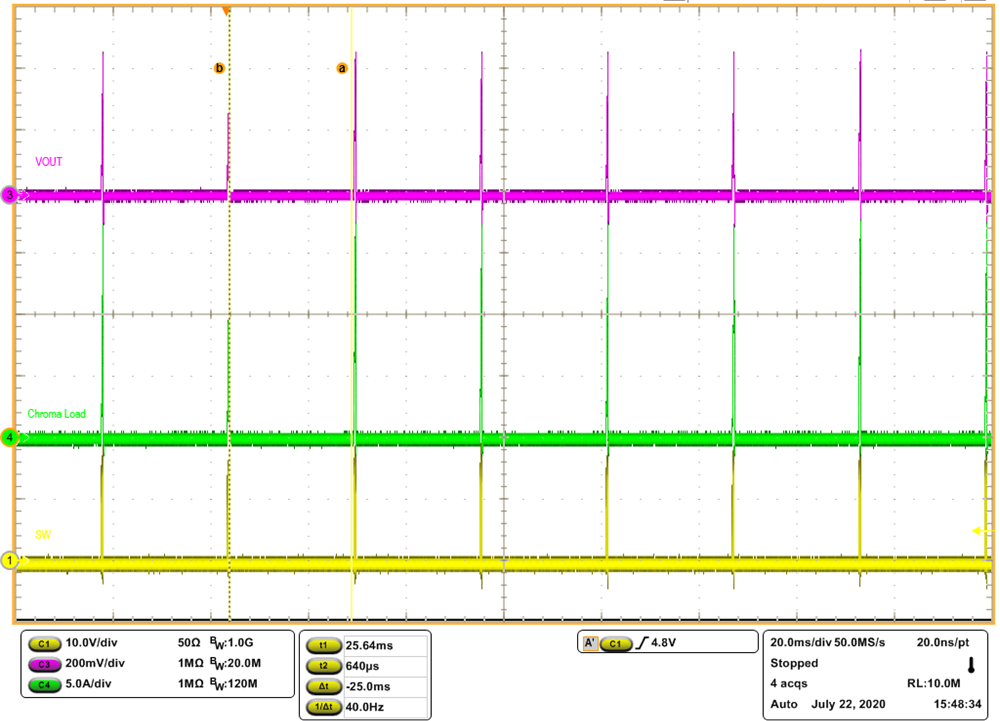
GUID-20200811-CA0I-0XL7-Q3JB-Z3K4KPVRG76T-low.png
VIN = 12 V VOUT = 1 V fSW = 1.0 MHz BOM
Figure 6-24 Short Overcurrent Protection Hiccup by Electronic Load
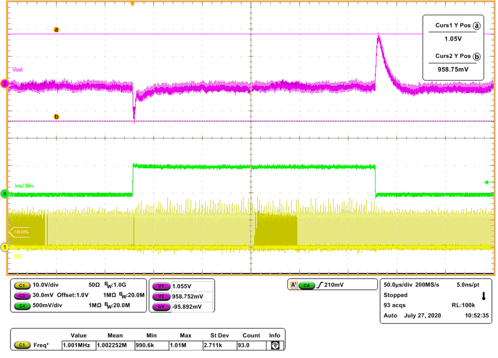
GUID-20200811-CA0I-QSRL-W2BP-DT0F67JGXGQB-low.png
VIN = 12 V VOUT = 1 V fSW = 1.0 MHz BOM
Figure 6-26 Load Transient 2 A to 12 A to 2 A at 20 A/μs