ZHCSTR3B December 2010 – November 2023 TPS53315
PRODUCTION DATA
- 1
- 1 特性
- 2 应用
- 3 说明
- 4 Pin Configuration and Functions
- 5 Specifications
-
6 Detailed Description
- 6.1 Overview
- 6.2 Functional Block Diagram
- 6.3
Feature Description
- 6.3.1 D-CAP™ Integrated Circuit with Adaptive On-Time
- 6.3.2 Small Signal Model
- 6.3.3 Ramp Signal
- 6.3.4 Auto-Skip Eco-mode Light Load Operation
- 6.3.5 Adaptive Zero Crossing
- 6.3.6 Forced Continuous Conduction Mode
- 6.3.7 Power Good
- 6.3.8 Current Sense and Overcurrent Protection
- 6.3.9 Overvoltage and Undervoltage Protection
- 6.3.10 UVLO Protection
- 6.3.11 Thermal Shutdown
- 6.4 Device Functional Modes
-
7 Application and Implementation
- 7.1 Application Information
- 7.2
Typical Application
- 7.2.1
Typical Application Circuit Diagram
- 7.2.1.1 Design Requirements
- 7.2.1.2
Detailed Design Procedure
- 7.2.1.2.1 Step 1: Select Operation Mode and Soft-Start Time
- 7.2.1.2.2 Step 2: Select Switching Frequency
- 7.2.1.2.3 Step 3: Select the Inductance
- 7.2.1.2.4 Step 4: Select Output Capacitors
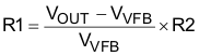
- 7.2.1.2.5 Step 5: Determine the Voltage-Divider Resistance (R1 and R2)
- 7.2.1.2.6 Step 6: Select the Overcurrent Resistance (RTRIP)
- 7.2.1.3 Application Curves
- 7.2.2 Typical Application Circuit Diagram With Ceramic Output Capacitors
- 7.2.1
Typical Application Circuit Diagram
- 7.3 Power Supply Recommendations
- 7.4 Layout
- 8 Device and Documentation Support
- 9 Revision History
- 10Mechanical, Packaging, and Orderable Information
7.2.2.3 External Component Selection When Using All Ceramic Output Capacitors
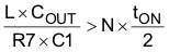
When a ceramic output capacitor is used, the stability criteria in Equation 2 cannot be satisfied. The ripple injection approach as shown in Figure 7-4 is implemented to increase the ripple on the VFB pin and make the system stable. In addition to the selections made using Section 7.2.2.2.1 through Section 7.2.2.2.5, use the information in the Section 7.2.2.3 section to select the ripple injection components. The C2 value can be fixed at 1 nF. Select a value for C1 between 10 nF and 200 nF.
where
- N is the coefficient to account for L and COUT variation.
N is also used to provide enough margin for stability. TI recommends N = 2 for VOUT ≤ 1.8 V and N = 4 for VOUT ≥ 3.3 V or when L ≤ 250 nH. The higher VOUT needs a higher N value because the effective output capacitance is reduced significantly with higher DC bias. For example, a 6.3-V, 22-µF ceramic capacitor can have only 8 µF of effective capacitance when biased at 5 V.
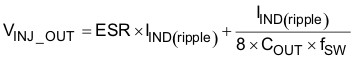
Because the VFB pin voltage is regulated at the valley, the increased ripple on the VFB pin causes the increase of the VFB DC value. The AC ripple coupled to the VFB pin has two components, one coupled from SW node and the other coupled from the VOUT pin and they can be calculated using Equation 15 and Equation 16 when neglecting the output voltage ripple caused by equivalent series inductance (ESL).
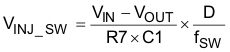
TI recommends that VINJ_SW to be less than 50 mV. If the calculated VINJ_SW is higher than 50 mV, then other parameters must be adjusted to reduce it. For example, COUT can be increased to satisfy Equation 14 with a higher R7 value, thereby reducing VINJ_SW.
The DC voltage at the VFB pin can be calculated by Equation 17:
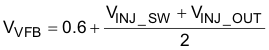
And the resistor divider value can be determined by Equation 18: