ZHCSTR3B December 2010 – November 2023 TPS53315
PRODUCTION DATA
- 1
- 1 特性
- 2 应用
- 3 说明
- 4 Pin Configuration and Functions
- 5 Specifications
-
6 Detailed Description
- 6.1 Overview
- 6.2 Functional Block Diagram
- 6.3
Feature Description
- 6.3.1 D-CAP™ Integrated Circuit with Adaptive On-Time
- 6.3.2 Small Signal Model
- 6.3.3 Ramp Signal
- 6.3.4 Auto-Skip Eco-mode Light Load Operation
- 6.3.5 Adaptive Zero Crossing
- 6.3.6 Forced Continuous Conduction Mode
- 6.3.7 Power Good
- 6.3.8 Current Sense and Overcurrent Protection
- 6.3.9 Overvoltage and Undervoltage Protection
- 6.3.10 UVLO Protection
- 6.3.11 Thermal Shutdown
- 6.4 Device Functional Modes
-
7 Application and Implementation
- 7.1 Application Information
- 7.2
Typical Application
- 7.2.1
Typical Application Circuit Diagram
- 7.2.1.1 Design Requirements
- 7.2.1.2
Detailed Design Procedure
- 7.2.1.2.1 Step 1: Select Operation Mode and Soft-Start Time
- 7.2.1.2.2 Step 2: Select Switching Frequency
- 7.2.1.2.3 Step 3: Select the Inductance
- 7.2.1.2.4 Step 4: Select Output Capacitors
- 7.2.1.2.5 Step 5: Determine the Voltage-Divider Resistance (R1 and R2)
- 7.2.1.2.6 Step 6: Select the Overcurrent Resistance (RTRIP)
- 7.2.1.3 Application Curves
- 7.2.2 Typical Application Circuit Diagram With Ceramic Output Capacitors
- 7.2.1
Typical Application Circuit Diagram
- 7.3 Power Supply Recommendations
- 7.4 Layout
- 8 Device and Documentation Support
- 9 Revision History
- 10Mechanical, Packaging, and Orderable Information
6.3.1 D-CAP™ Integrated Circuit with Adaptive On-Time
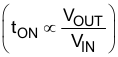
The TPS53315 does not have a dedicated oscillator to determine switching frequency. However, the device operates with pseudo-constant frequency by feed-forwarding the input and output voltages into the on-time one-shot timer. The adaptive on-time control adjusts the on-time to be inversely proportional to the input voltage and proportional to the output voltage
 .
.
This makes the switching frequency fairly constant in steady state conditions over a wide input voltage range. The switching frequency is selectable from eight preset values by a resistor connected between the RF pin and GND or between the RF pin and the VREG pin as shown in Table 6-1. Leaving the resistance open sets the switching frequency to 500 kHz.
| RESISTOR (RRF) CONNECTIONS | SWITCHING FREQUENCY (kHz) |
|---|---|
| 0 Ω to GND | 250 |
| 187 kΩ to GND | 300 |
| 619 kΩ to GND | 400 |
| Open | 500 |
| 866 kΩ to VREG | 600 |
| 309 kΩ to VREG | 750 |
| 124 kΩ to VREG | 850 |
| 0 Ω to VREG | 970 |
The off-time is modulated by a PWM comparator. The VFB node voltage (the mid-point of resistor divider) is compared to the internal 0.6-V reference voltage added with a ramp signal. When the signal values match, the PWM comparator asserts a set signal to terminate the off-time (turn off the low-side MOSFET and turn on high-side MOSFET). The set signal is valid if the inductor current level is below the OCP threshold, otherwise the off-time is extended until the current level falls below the threshold.
Figure 6-1 and Figure 6-2 show two on-time control schemes.
 Figure 6-1 On-Time Control Without Ramp Compensation
 Figure 6-2 On-Time Control With Ramp Compensation