ZHCSTR3B December 2010 – November 2023 TPS53315
PRODUCTION DATA
- 1
- 1 特性
- 2 应用
- 3 说明
- 4 Pin Configuration and Functions
- 5 Specifications
-
6 Detailed Description
- 6.1 Overview
- 6.2 Functional Block Diagram
- 6.3
Feature Description
- 6.3.1 D-CAP™ Integrated Circuit with Adaptive On-Time
- 6.3.2 Small Signal Model
- 6.3.3 Ramp Signal
- 6.3.4 Auto-Skip Eco-mode Light Load Operation
- 6.3.5 Adaptive Zero Crossing
- 6.3.6 Forced Continuous Conduction Mode
- 6.3.7 Power Good
- 6.3.8 Current Sense and Overcurrent Protection
- 6.3.9 Overvoltage and Undervoltage Protection
- 6.3.10 UVLO Protection
- 6.3.11 Thermal Shutdown
- 6.4 Device Functional Modes
-
7 Application and Implementation
- 7.1 Application Information
- 7.2
Typical Application
- 7.2.1
Typical Application Circuit Diagram
- 7.2.1.1 Design Requirements
- 7.2.1.2
Detailed Design Procedure
- 7.2.1.2.1 Step 1: Select Operation Mode and Soft-Start Time
- 7.2.1.2.2 Step 2: Select Switching Frequency
- 7.2.1.2.3 Step 3: Select the Inductance
- 7.2.1.2.4 Step 4: Select Output Capacitors
- 7.2.1.2.5 Step 5: Determine the Voltage-Divider Resistance (R1 and R2)
- 7.2.1.2.6 Step 6: Select the Overcurrent Resistance (RTRIP)
- 7.2.1.3 Application Curves
- 7.2.2 Typical Application Circuit Diagram With Ceramic Output Capacitors
- 7.2.1
Typical Application Circuit Diagram
- 7.3 Power Supply Recommendations
- 7.4 Layout
- 8 Device and Documentation Support
- 9 Revision History
- 10Mechanical, Packaging, and Orderable Information
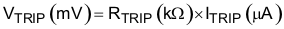
6.3.8 Current Sense and Overcurrent Protection
TPS53315 has cycle-by-cycle overcurrent limiting control. The inductor current is monitored during the OFF state and the controller maintains the OFF state during the period in that the inductor current is larger than the overcurrent trip level. To provide both good accuracy and cost effective solution, TPS53315 supports temperature compensated MOSFET RDS(on) sensing. The TRIP pin must be connected to GND through the trip voltage setting resistor, RTRIP. The TRIP pin sources ITRIP current, which is 10 μA typically at room temperature, and the trip level is set to the OCL trip voltage VTRIP as shown in Equation 4.
The inductor current is monitored by the voltage between the GND pin and the SW pin so that the SW pin must be connected to the drain terminal of the low-side MOSFET properly. ITRIP has 4700 ppm/°C temperature slope to compensate the temperature dependency of the RDS(on). The GND pin is used as the positive current sensing node. The GND pin must be connected to the proper current sensing device, (for example, the source terminal of the low-side MOSFET.)
As the comparison is done during the OFF state, VTRIP sets the valley level of the inductor current. Thus, the load current at the overcurrent threshold, IOCP, can be calculated as shown in Equation 5.

In an overcurrent condition, the current to the load exceeds the current to the output capacitor, therefore the output voltage tends to decrease. Eventually, it crosses the undervoltage protection threshold and shuts down. After a hiccup delay (16 ms with 0.7-ms sort-start), the controller restarts. If the overcurrent condition remains, the procedure is repeated and the device enters hiccup mode.
During CCM, the negative current limit (NCL) protects the internal FET from carrying too much current. The NCL detect threshold is set as the same absolute value as positive OCL but negative polarity. Note that the threshold continues to represent the valley value of the inductor current.