ZHCSTR3B December 2010 – November 2023 TPS53315
PRODUCTION DATA
- 1
- 1 特性
- 2 应用
- 3 说明
- 4 Pin Configuration and Functions
- 5 Specifications
-
6 Detailed Description
- 6.1 Overview
- 6.2 Functional Block Diagram
- 6.3
Feature Description
- 6.3.1 D-CAP™ Integrated Circuit with Adaptive On-Time
- 6.3.2 Small Signal Model
- 6.3.3 Ramp Signal
- 6.3.4 Auto-Skip Eco-mode Light Load Operation
- 6.3.5 Adaptive Zero Crossing
- 6.3.6 Forced Continuous Conduction Mode
- 6.3.7 Power Good
- 6.3.8 Current Sense and Overcurrent Protection
- 6.3.9 Overvoltage and Undervoltage Protection
- 6.3.10 UVLO Protection
- 6.3.11 Thermal Shutdown
- 6.4 Device Functional Modes
-
7 Application and Implementation
- 7.1 Application Information
- 7.2
Typical Application
- 7.2.1
Typical Application Circuit Diagram
- 7.2.1.1 Design Requirements
- 7.2.1.2
Detailed Design Procedure
- 7.2.1.2.1 Step 1: Select Operation Mode and Soft-Start Time
- 7.2.1.2.2 Step 2: Select Switching Frequency
- 7.2.1.2.3 Step 3: Select the Inductance
- 7.2.1.2.4 Step 4: Select Output Capacitors
- 7.2.1.2.5 Step 5: Determine the Voltage-Divider Resistance (R1 and R2)
- 7.2.1.2.6 Step 6: Select the Overcurrent Resistance (RTRIP)
- 7.2.1.3 Application Curves
- 7.2.2 Typical Application Circuit Diagram With Ceramic Output Capacitors
- 7.2.1
Typical Application Circuit Diagram
- 7.3 Power Supply Recommendations
- 7.4 Layout
- 8 Device and Documentation Support
- 9 Revision History
- 10Mechanical, Packaging, and Orderable Information
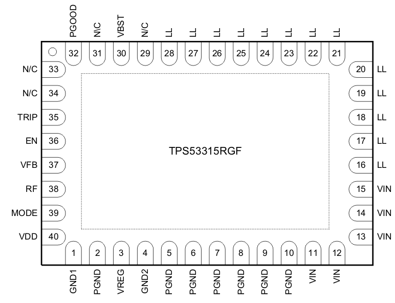
4 Pin Configuration and Functions
 Figure 4-1 RGF Package40-Pin VQFN With Exposed
Thermal PadTop View
Figure 4-1 RGF Package40-Pin VQFN With Exposed
Thermal PadTop ViewTable 4-1 Pin Functions
| PIN | TYPE(1) | DESCRIPTION | ||
|---|---|---|---|---|
| NAME | NO. | |||
| EN | 36 | I | Enable pin | |
| GND1 | 1 | G | GND for controller | |
| GND2 | 4 | G | GND for half-bridge | |
| LL | 16 | B | Output of converted power; connect this pin to the output inductor. | |
| 17 | ||||
| 18 | ||||
| 19 | ||||
| 20 | ||||
| 21 | ||||
| 22 | ||||
| 23 | ||||
| 24 | ||||
| 25 | ||||
| 26 | ||||
| 27 | ||||
| 28 | ||||
| MODE | 39 | I | Soft-start and skip/CCM selection; connect a resistor to select soft-start time using Table 6-2. The soft-start time is detected and stored into internal register during start-up. | |
| N/C | 29 | No connection | ||
| 31 | ||||
| 33 | ||||
| 34 | ||||
| PGOOD | 32 | O | Open drain power good flag provides a 1-ms start up delay after the VFB pin voltage falls within specified limits. When the VFB pin voltage goes outside the specified limits, the PGOOD pin goes low within 10 µs. | |
| PGND | 2 | G | Power GND | |
| 5 | ||||
| 6 | ||||
| 7 | ||||
| 8 | ||||
| 9 | ||||
| 10 | ||||
| RF | 38 | I | Switching frequency selection. Connect a resistance to GND or VREG to select switching frequency using Table 6-1. The switching frequency is detected and stored during the startup. | |
| TRIP | 35 | I | OCL detection threshold setting pin, 10 µA at room temperature, 4700 ppm/°C current is sourced and set the OCL trip voltage as follows: | |
| VOCL = VTRIP/8 | (VTRIP ≤ 1.2 V, VOCL ≤ 150 mV) | |||
| VBST | 30 | P | Supply input for high-side FET gate driver (boost terminal); connect capacitor from this pin to LL-node. Internally connected to the VREG pin through bootstrap MOSFET switch. | |
| VDD | 40 | P | Controller power supply input | |
| VFB | 37 | I | Output feedback input; connect this pin to VOUT through a resistor divider. | |
| VIN | 11 | P | Conversion power input | |
| 12 | ||||
| 13 | ||||
| 14 | ||||
| 15 | ||||
| VREG | 3 | P | 5-V LDO output | |
(1) I = Input, O = Output, B = Bidirectional, G = Ground, P =
Supply