ZHCS155C March 2011 – November 2023 TPS40170
PRODUCTION DATA
- 1
- 1 特性
- 2 应用
- 3 说明
- 4 Pin Configuration and Functions
- 5 Specifications
-
6 Detailed Description
- 6.1 Overview
- 6.2 Functional Block Diagram
- 6.3
Feature Description
- 6.3.1 LDO Linear Regulators and Enable
- 6.3.2 Input Undervoltage Lockout (UVLO)
- 6.3.3 Oscillator and Voltage Feed-Forward
- 6.3.4 Overcurrent Protection and Short-Circuit Protection (OCP and SCP)
- 6.3.5 Soft-Start and Fault-Logic
- 6.3.6 Overtemperature Fault
- 6.3.7 Tracking
- 6.3.8 Adaptive Drivers
- 6.3.9 Start-Up into Pre-Biased Output
- 6.3.10 Power Good (PGOOD)
- 6.3.11 PGND and AGND
- 6.4 Device Functional Modes
-
7 Application and Implementation
- 7.1 Application Information
- 7.2
Typical Application
- 7.2.1 Design Requirements
- 7.2.2
Detailed Design Procedure
- 7.2.2.1 Custom Design with WEBENCH® Tools
- 7.2.2.2 List of Materials
- 7.2.2.3 Select a Switching Frequency
- 7.2.2.4 Inductor Selection (L1)
- 7.2.2.5 Output Capacitor Selection (C9)
- 7.2.2.6 Peak Current Rating of Inductor
- 7.2.2.7 Input Capacitor Selection (C1, C6)
- 7.2.2.8 MOSFET Switch Selection (Q1, Q2)
- 7.2.2.9 Timing Resistor (R7)
- 7.2.2.10 UVLO Programming Resistors (R2, R6)
- 7.2.2.11 Boot-Strap Capacitor (C7)
- 7.2.2.12 VIN Bypass Capacitor (C18)
- 7.2.2.13 VBP Bypass Capacitor (C19)
- 7.2.2.14 VDD Bypass Capacitor (C16)
- 7.2.2.15 SS Timing Capacitor (C15)
- 7.2.2.16 ILIM Resistor (R9, C17)
- 7.2.2.17 SCP Multiplier Selection (R5)
- 7.2.2.18 Feedback Divider (R10, R11)
- 7.2.2.19 Compensation: (R4, R13, C13, C14, C21)
- 7.2.3 Application Curves
- 7.3 Power Supply Recommendations
- 7.4 Layout
- 8 Device and Documentation Support
- 9 Revision History
- 10Mechanical, Packaging, and Orderable Information
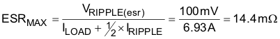
7.2.2.7 Input Capacitor Selection (C1, C6)
The input voltage ripple is divided between capacitance and ESR. For this design VRIPPLE(cap) = 400 mV and VRIPPLE(ESR) = 100 mV. The minimum capacitance and maximum ESR are estimated by:
Equation 27.
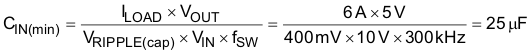
Equation 28.
The RMS current in the input capacitors is estimated in Equation 29.
Equation 29.

To achieve these values, four 1210, 2.2 µF, 100 V, X7R ceramic capacitors plus a 120 µF electrolytic capacitor are combined at the input. This provides a smaller size and overall cost than 10 ceramic input capacitors or an electrolytic capacitor with the ESR required.
Table 7-3 Inductor Summary
| PARAMETER | VALUE | UNIT | |
|---|---|---|---|
| L | Inductance | 8.2 | µH |
| IL(rms) | RMS current (thermal rating) | 6.02 | A |
| IL(peak) | Peak current (saturation rating) | 7.01 | A |