ZHCS155C March 2011 – November 2023 TPS40170
PRODUCTION DATA
- 1
- 1 特性
- 2 应用
- 3 说明
- 4 Pin Configuration and Functions
- 5 Specifications
-
6 Detailed Description
- 6.1 Overview
- 6.2 Functional Block Diagram
- 6.3
Feature Description
- 6.3.1 LDO Linear Regulators and Enable
- 6.3.2 Input Undervoltage Lockout (UVLO)
- 6.3.3 Oscillator and Voltage Feed-Forward
- 6.3.4 Overcurrent Protection and Short-Circuit Protection (OCP and SCP)
- 6.3.5 Soft-Start and Fault-Logic
- 6.3.6 Overtemperature Fault
- 6.3.7 Tracking
- 6.3.8 Adaptive Drivers
- 6.3.9 Start-Up into Pre-Biased Output
- 6.3.10 Power Good (PGOOD)
- 6.3.11 PGND and AGND
- 6.4 Device Functional Modes
-
7 Application and Implementation
- 7.1 Application Information
- 7.2
Typical Application
- 7.2.1 Design Requirements
- 7.2.2
Detailed Design Procedure
- 7.2.2.1 Custom Design with WEBENCH® Tools
- 7.2.2.2 List of Materials
- 7.2.2.3 Select a Switching Frequency
- 7.2.2.4 Inductor Selection (L1)
- 7.2.2.5 Output Capacitor Selection (C9)
- 7.2.2.6 Peak Current Rating of Inductor
- 7.2.2.7 Input Capacitor Selection (C1, C6)
- 7.2.2.8 MOSFET Switch Selection (Q1, Q2)
- 7.2.2.9 Timing Resistor (R7)
- 7.2.2.10 UVLO Programming Resistors (R2, R6)
- 7.2.2.11 Boot-Strap Capacitor (C7)
- 7.2.2.12 VIN Bypass Capacitor (C18)
- 7.2.2.13 VBP Bypass Capacitor (C19)
- 7.2.2.14 VDD Bypass Capacitor (C16)
- 7.2.2.15 SS Timing Capacitor (C15)
- 7.2.2.16 ILIM Resistor (R9, C17)
- 7.2.2.17 SCP Multiplier Selection (R5)
- 7.2.2.18 Feedback Divider (R10, R11)
- 7.2.2.19 Compensation: (R4, R13, C13, C14, C21)
- 7.2.3 Application Curves
- 7.3 Power Supply Recommendations
- 7.4 Layout
- 8 Device and Documentation Support
- 9 Revision History
- 10Mechanical, Packaging, and Orderable Information
7.2.2 Detailed Design Procedure
Equation 19.
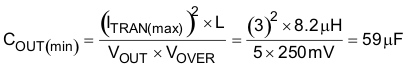
With a minimum capacitance, the maximum allowable ESR is determined by the maximum ripple voltage and is approximated Equation 20.
Equation 20.

Two 1210, 22 µF, 16 V X7R ceramic capacitors plus two 0805 10 µF, 16 V X7R ceramic capacitors are selected to provide more than 59 µF of minimum capacitance (including tolerance and DC bias derating) and less than 47 mΩ of ESR (parallel ESR of approximately 4 mΩ).