ZHCS155C March 2011 – November 2023 TPS40170
PRODUCTION DATA
- 1
- 1 特性
- 2 应用
- 3 说明
- 4 Pin Configuration and Functions
- 5 Specifications
-
6 Detailed Description
- 6.1 Overview
- 6.2 Functional Block Diagram
- 6.3
Feature Description
- 6.3.1 LDO Linear Regulators and Enable
- 6.3.2 Input Undervoltage Lockout (UVLO)
- 6.3.3 Oscillator and Voltage Feed-Forward
- 6.3.4 Overcurrent Protection and Short-Circuit Protection (OCP and SCP)
- 6.3.5 Soft-Start and Fault-Logic
- 6.3.6 Overtemperature Fault
- 6.3.7 Tracking
- 6.3.8 Adaptive Drivers
- 6.3.9 Start-Up into Pre-Biased Output
- 6.3.10 Power Good (PGOOD)
- 6.3.11 PGND and AGND
- 6.4 Device Functional Modes
-
7 Application and Implementation
- 7.1 Application Information
- 7.2
Typical Application
- 7.2.1 Design Requirements
- 7.2.2
Detailed Design Procedure
- 7.2.2.1 Custom Design with WEBENCH® Tools
- 7.2.2.2 List of Materials
- 7.2.2.3 Select a Switching Frequency
- 7.2.2.4 Inductor Selection (L1)
- 7.2.2.5 Output Capacitor Selection (C9)
- 7.2.2.6 Peak Current Rating of Inductor
- 7.2.2.7 Input Capacitor Selection (C1, C6)
- 7.2.2.8 MOSFET Switch Selection (Q1, Q2)
- 7.2.2.9 Timing Resistor (R7)
- 7.2.2.10 UVLO Programming Resistors (R2, R6)
- 7.2.2.11 Boot-Strap Capacitor (C7)
- 7.2.2.12 VIN Bypass Capacitor (C18)
- 7.2.2.13 VBP Bypass Capacitor (C19)
- 7.2.2.14 VDD Bypass Capacitor (C16)
- 7.2.2.15 SS Timing Capacitor (C15)
- 7.2.2.16 ILIM Resistor (R9, C17)
- 7.2.2.17 SCP Multiplier Selection (R5)
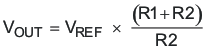
- 7.2.2.18 Feedback Divider (R10, R11)
- 7.2.2.19 Compensation: (R4, R13, C13, C14, C21)
- 7.2.3 Application Curves
- 7.3 Power Supply Recommendations
- 7.4 Layout
- 8 Device and Documentation Support
- 9 Revision History
- 10Mechanical, Packaging, and Orderable Information
6.3.5 Soft-Start and Fault-Logic
A capacitor from the SS pin to GND defines the SS time, tSS. The TPS40170 enters into soft-start immediately after completion of the overcurrent calibration. The SS pin goes through the device internal level-shifter circuit before reaching one of the positive inputs of the error amplifier. The SS pin must reach approximately 0.65 V before the input to the error amplifier begins to rise above 0 V. To charge the SS pin from 0 V to 0.65 V faster, at the beginning of the soft-start in addition to the normal charging current, (11.6 µA, typ.), an extra charging current (40.4 µA, typ.) is switched-in to the SS pin. As the SS capacitor reaches 0.5 V, the extra charging current is turned off and only the normal charging current remains. Figure 6-5 shows the soft-start function block.
 Figure 6-5 Soft-Start Schematic Block
As the SS pin voltage approaches 0.65 V, the positive input to the error amplifier begins to rise (see Figure 6-6). The output of the error amplifier (the COMP pin) starts rising. The rate of rise of the COMP voltage is mainly limited by the feedback loop compensation network. After VCOMP reaches the valley of the PWM ramp, the switching begins. The output is regulated to the error amplifier input through the FB pin in the feedback loop. After the FB pin reaches the 600 mV reference voltage, the feedback node is regulated to the reference voltage, VREF. The SS pin continues to rise and is clamped to VDD.
The SS pin is discharged through an internal switch during the following conditions:
- Input (VIN) undervoltage lock out UVLO pin less than VUVLO
- Overcurrent protection calibration time (tCAL)
- VBP less than threshold voltage (VBP(off))
Because it is discharged through an internal switch, the discharging time is relatively fast compared with the discharging time during the fault restart which is discussed in the Soft-Start During Overcurrent Fault section.
 Figure 6-6 Soft-Start Waveforms
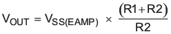
Referring to Figure 6-6
- (1) VREF dominates the positive input of the error amplifier
- (2) SS_EAMP dominates the positive input of the error amplifier
For 0 < VSS_EAMP < VREF
For VSS_EAMP > VREF