ZHCS155C March 2011 – November 2023 TPS40170
PRODUCTION DATA
- 1
- 1 特性
- 2 应用
- 3 说明
- 4 Pin Configuration and Functions
- 5 Specifications
-
6 Detailed Description
- 6.1 Overview
- 6.2 Functional Block Diagram
- 6.3
Feature Description
- 6.3.1 LDO Linear Regulators and Enable
- 6.3.2 Input Undervoltage Lockout (UVLO)
- 6.3.3 Oscillator and Voltage Feed-Forward
- 6.3.4 Overcurrent Protection and Short-Circuit Protection (OCP and SCP)
- 6.3.5 Soft-Start and Fault-Logic
- 6.3.6 Overtemperature Fault
- 6.3.7 Tracking
- 6.3.8 Adaptive Drivers
- 6.3.9 Start-Up into Pre-Biased Output
- 6.3.10 Power Good (PGOOD)
- 6.3.11 PGND and AGND
- 6.4 Device Functional Modes
-
7 Application and Implementation
- 7.1 Application Information
- 7.2
Typical Application
- 7.2.1 Design Requirements
- 7.2.2
Detailed Design Procedure
- 7.2.2.1 Custom Design with WEBENCH® Tools
- 7.2.2.2 List of Materials
- 7.2.2.3 Select a Switching Frequency
- 7.2.2.4 Inductor Selection (L1)
- 7.2.2.5 Output Capacitor Selection (C9)
- 7.2.2.6 Peak Current Rating of Inductor
- 7.2.2.7 Input Capacitor Selection (C1, C6)
- 7.2.2.8 MOSFET Switch Selection (Q1, Q2)
- 7.2.2.9 Timing Resistor (R7)
- 7.2.2.10 UVLO Programming Resistors (R2, R6)
- 7.2.2.11 Boot-Strap Capacitor (C7)
- 7.2.2.12 VIN Bypass Capacitor (C18)
- 7.2.2.13 VBP Bypass Capacitor (C19)
- 7.2.2.14 VDD Bypass Capacitor (C16)
- 7.2.2.15 SS Timing Capacitor (C15)
- 7.2.2.16 ILIM Resistor (R9, C17)
- 7.2.2.17 SCP Multiplier Selection (R5)
- 7.2.2.18 Feedback Divider (R10, R11)
- 7.2.2.19 Compensation: (R4, R13, C13, C14, C21)
- 7.2.3 Application Curves
- 7.3 Power Supply Recommendations
- 7.4 Layout
- 8 Device and Documentation Support
- 9 Revision History
- 10Mechanical, Packaging, and Orderable Information
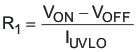
6.3.2.1 Equations for Programming the Input UVLO:
Components R1 and R2 represent external resistors for programming UVLO and hysteresis and can be calculated in Equation 1 and Equation 2 respectively.
Equation 1.
Equation 26.
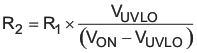
where
- VON is the desired turn-on voltage of the converter
- VOFF is the desired turn-off voltage for the converter
- IUVLO is the hysteresis current generated by the device, 5.0 µA (typ)
- VUVLO is the UVLO pin threshold voltage, 0.9 V (typ)
Note:
If the UVLO pin is connected to a voltage greater than 0.9 V, the programmable UVLO is disabled and the device defaults to an internal UVLO (VBP(on) and VBP(off)). For example, the UVLO pin can be connected to VDD or the VBP pin to disable the programmable UVLO function.
A 1 nF ceramic by-pass capacitor must be connected between the UVLO pin and GND.