ZHCSO95B june 2022 – may 2023 TPS1641
PRODUCTION DATA
- 1
- 1 特性
- 2 应用
- 3 说明
- 4 Revision History
- 5 Device Comparison Table
- 6 Pin Configuration and Functions
- 7 Specifications
-
8 Detailed Description
- 8.1 Overview
- 8.2 Functional Block Diagram
- 8.3
Feature Description
- 8.3.1 Enable and Shutdown Input (EN/SHDN)
- 8.3.2 Overvoltage Protection (OVP)
- 8.3.3 Output Slew Rate and Inrush Current Control (dVdt)
- 8.3.4 Active Current Limiting (ILIM) With the TPS16412, TPS16413, TPS16416, and TPS16417
- 8.3.5 Active Power Limiting (PLIM) With the TPS16410, TPS16411, TPS16414, and TPS16415
- 8.3.6 Overcurrent Protection (IOCP) and Blanking Time (IDLY or PDLY) for Transient Loads
- 8.3.7 Fast-Trip and Short-Circuit Protection
- 8.3.8 Analog Load Current Monitor (IMON) on the IOCP Pin
- 8.3.9 IN to OUT Short Detection (TPS16410, TPS16411, TPS16412, and TPS16413)
- 8.3.10 Thermal Shutdown and Overtemperature Protection
- 8.3.11 Fault Response and Indication (FLT)
- 8.4 Device Functional Modes
- 9 Application and Implementation
- 10Device and Documentation Support
- 11Mechanical, Packaging, and Orderable Information
8.3.3 Output Slew Rate and Inrush Current Control (dVdt)
During hot plug events or while trying to charge a large output capacitance, there can be a large inrush current. If the inrush current is not managed properly, it can damage the input connectors and cause the system power supply to droop leading to unexpected restarts elsewhere in the system. The inrush current during turn-on is directly proportional to the load capacitance and rising slew rate. Equation 1 can be used to find the output slew rate (SR) required to limit the inrush current (IINRUSH) for a given output capacitance (COUT).
A capacitance can be added to the dVdt pin to control the rising slew rate and lower the inrush current during turn-on. The required CdVdt capacitance to produce a given slew rate can be calculated using Equation 2.
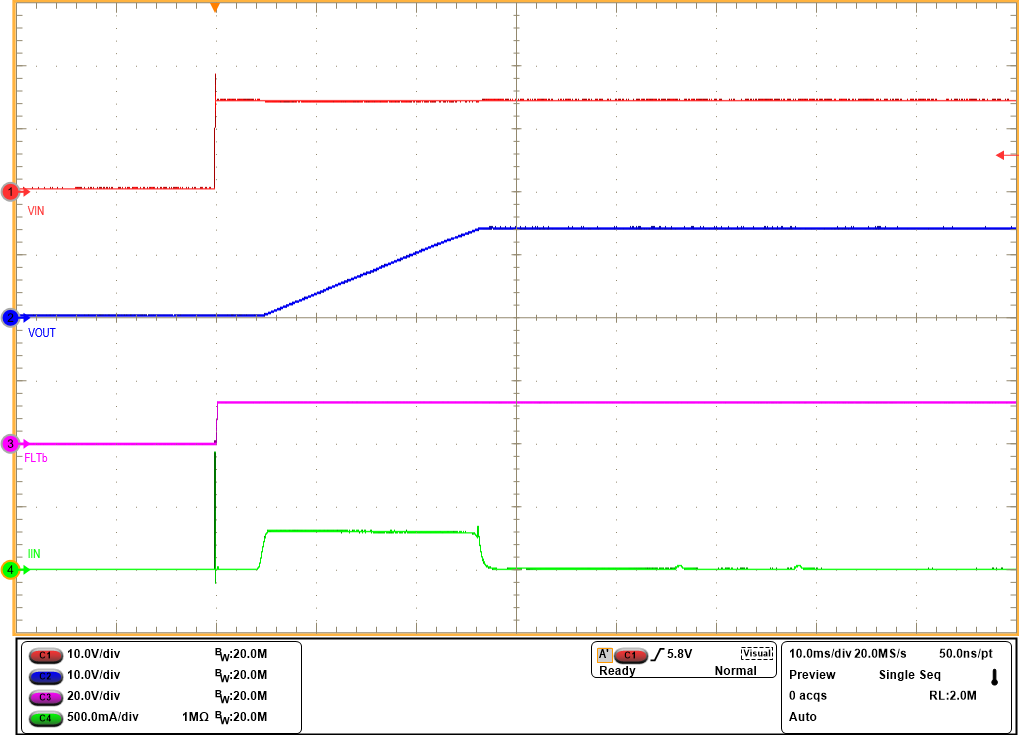
The fastest output slew rate is achieved by leaving the dVdt pin open. If dVdt pin is connected to GND, the device will not power up the output. Figure 8-8 illustrates the output slew rate control in the TPS1641x devices. Figure 8-9 shows the output slew rate control response of the device.
 Figure 8-8 Output Slew Rate Control in
the TPS1641x
 Figure 8-9 Output Slew Rate Control with
VIN = 12 V, CdVdt = 150 nF, and COUT = 470
μF