ZHCSQQ4C November 2011 – June 2022 TPA2015D1
PRODUCTION DATA
- 1 特性
- 2 应用
- 3 说明
- 4 Revision History
- 5 Device Comparison Table
- 6 Pin Configuration and Functions
- 7 Specifications
- 8 Parameter Measurement Information
-
9 Detailed Description
- 9.1 Overview
- 9.2 Functional Block Diagram
- 9.3 Feature Description
- 9.4 Device Functional Modes
- 10Application and Implementation
- 11Power Supply Recommendations
- 12Layout
- 13Device and Documentation Support
- 14Mechanical, Packaging, and Orderable Information
9.3.3 Adaptive Boost Converter
The TPA2015D1 consists of an adaptive boost converter and a Class-D amplifier. The boost converter takes the supply voltage, VBAT, and increases it to a higher output voltage, PVOUT. PVOUT drives the supply voltage of the Class-D amplifier, PVDD. This improves loudness over non-boosted solutions.
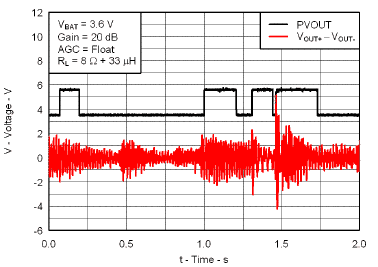
The boost converter is adaptive and activates automatically depending on the output audio signal amplitude. When the peak output audio signal exceeds a preset voltage threshold, the boost converter is enabled, and the voltage at PVOUT is 5.5 V. When the audio output voltage is lower than the threshold voltage, the boost deactivates automatically. The boost activation threshold voltage is not user programmable. It is optimized to prevent clipping while maximizing system efficiency.
The boost converter can be forcibly deactivated by setting the ENB pin to logic-low. When the boost is deactivated, PVOUT is equal to the supply voltage (VBAT) minus the I x R drop across the inductor and boost converter pass transistor.
A timer prevents the input signal from modulating the PVOUT voltage within the audio frequency range, eliminating the potential for audible artifacts on the Class-D output.
Figure 9-5 shows how the adaptive boost modulates with a typical audio signal. By automatically deactivating the boost converter and passing VBAT to PVOUT, the TPA2015D1 efficiency is improved at low output power.

The primary external components for the boost converter are the inductor and the boost capacitor. The inductor stores current, and the boost capacitor stores charge. As the Class-D amplifier depletes the charge in the boost capacitor, the boost inductor replenishes charge with its stored current. The cycle of charge and discharge occurs frequently enough to keep PVOUT within its minimum and maximum voltage specification.
The boost converter design is optimized for driving the integrated Class-D amplifier only. It lacks protection circuitry recommended for driving loads other than the integrated Class-D amplifier.