ZHCSQQ4C November   2011  – June 2022 TPA2015D1

PRODUCTION DATA  

  1. 特性
  2. 应用
  3. 说明
  4. Revision History
  5. Device Comparison Table
  6. Pin Configuration and Functions
  7. Specifications
    1. 7.1 Absolute Maximum Ratings
    2. 7.2 ESD Ratings
    3. 7.3 Recommended Operating Conditions
    4. 7.4 Thermal Information
    5. 7.5 Electrical Characteristics
    6. 7.6 Operating Characteristics
    7. 7.7 Typical Characteristics
  8. Parameter Measurement Information
  9. Detailed Description
    1. 9.1 Overview
    2. 9.2 Functional Block Diagram
    3. 9.3 Feature Description
      1. 9.3.1 SpeakerGuard™ Theory of Operation
        1. 9.3.1.1 SpeakerGuard™ With Varying Input Levels
        2. 9.3.1.2 Battery Tracking SpeakerGuard™
      2. 9.3.2 Fully Differential Class-D Amplifier
        1. 9.3.2.1 Advantages of Fully Differential Amplifiers
        2. 9.3.2.2 Improved Class-D Efficiency
      3. 9.3.3 Adaptive Boost Converter
        1. 9.3.3.1 Boost Converter Overvoltage Protection
      4. 9.3.4 Operation With DACs and CODECs
      5. 9.3.5 Filter Free Operation and Ferrite Bead Filters
      6. 9.3.6 Speaker Load Limitation
      7. 9.3.7 Fixed Gain Setting
    4. 9.4 Device Functional Modes
      1. 9.4.1 Shutdown Mode
      2. 9.4.2 Battery Tracking SpeakerGuard™ Operation
  10. 10Application and Implementation
    1. 10.1 Application Information
    2. 10.2 Typical Applications
      1. 10.2.1 TPA2015D1 With Differential Input Signals
        1. 10.2.1.1 Design Requirements
        2. 10.2.1.2 Detailed Design Procedure
          1. 10.2.1.2.1 Boost Converter Inductor Selection
            1. 10.2.1.2.1.1 Inductor Equations
          2. 10.2.1.2.2 Boost Converter Capacitor Selection
          3. 10.2.1.2.3 Components Location and Selection
            1. 10.2.1.2.3.1 Decoupling Capacitors
            2. 10.2.1.2.3.2 Input Capacitors
        3. 10.2.1.3 Application Curves
      2. 10.2.2 TPA2015D1 with Single-Ended Input Signals
        1. 10.2.2.1 Design Requirements
        2. 10.2.2.2 Detailed Design Procedure
        3. 10.2.2.3 Application Curves
  11. 11Power Supply Recommendations
    1. 11.1 Power Supply Decoupling Capacitors
  12. 12Layout
    1. 12.1 Layout Guidelines
      1. 12.1.1 Component Placement
      2. 12.1.2 Trace Width
      3. 12.1.3 Pad Size
    2. 12.2 Layout Example
  13. 13Device and Documentation Support
    1. 13.1 Device Support
      1. 13.1.1 Device Nomenclature
        1. 13.1.1.1 TPA2015D1 Glossary
        2. 13.1.1.2 Boost Terms
    2. 13.2 Community Resources
    3. 13.3 Trademarks
  14. 14Mechanical, Packaging, and Orderable Information
    1. 14.1 Package Option Addendum
      1. 14.1.1 Packaging Information
      2. 14.1.2 Tape and Reel Information

封装选项

机械数据 (封装 | 引脚)
散热焊盘机械数据 (封装 | 引脚)
订购信息

Improved Class-D Efficiency

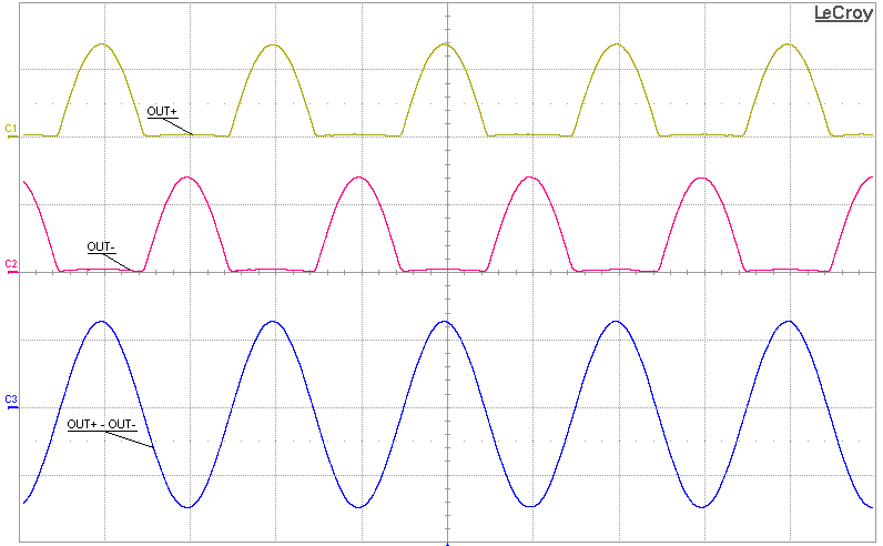
The TPA2015D1 output stage uses a modulation technique that modulates the PWM output only on one side of the differential output, leaving the other side held at ground. Although the differential output voltage is undistorted, each output appears as a half-wave rectified signal.

This technique reduces output switching losses and improves overall amplifier efficiency. Figure 9-4 shows how OUT+, OUT-, and the differential output voltages appear on an oscilloscope.
GUID-C6BA00CB-D193-4C66-9E5A-0EA9403B746D-low.png
C1(YELLOW) is OUT+C2(PINK) is OUT–C3(CYAN) is OUT+ - OUT–
Figure 9-4 Filtered Output Waveforms