ZHCSQQ4C November 2011 – June 2022 TPA2015D1
PRODUCTION DATA
- 1 特性
- 2 应用
- 3 说明
- 4 Revision History
- 5 Device Comparison Table
- 6 Pin Configuration and Functions
- 7 Specifications
- 8 Parameter Measurement Information
-
9 Detailed Description
- 9.1 Overview
- 9.2 Functional Block Diagram
- 9.3 Feature Description
- 9.4 Device Functional Modes
- 10Application and Implementation
- 11Power Supply Recommendations
- 12Layout
- 13Device and Documentation Support
- 14Mechanical, Packaging, and Orderable Information
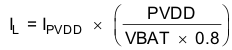
10.2.1.2.1.1 Inductor Equations
Inductor current rating is determined by the requirements of the load. The inductance is determined by two factors: the minimum value required for stability and the maximum ripple current permitted in the application.
Use Equation 1 to determine the required current rating. Equation 1 shows the approximate relationship between the average inductor current, IL, to the load current, load voltage, and input voltage (IPVDD, PVDD, and VBAT, respectively). Insert IPVDD, PVDD, and VBAT into Equation 1 and solve for IL. The inductor must maintain at least 90% of its initial inductance value at this current.
Use a minimum working inductance of 1.3 μH. Lower values may damage the inductor.
Use a minimum working inductance of 1.3 μH. Lower values may damage the inductor.
Ripple current, ΔIL, is peak-to-peak variation in inductor current. Smaller ripple current reduces core losses in the inductor and reduces the potential for EMI. Use Equation 2 to determine the value of the inductor, L. Equation 2 shows the relationship between inductance L, VBAT, PVDD, the switching frequency, fBOOST, and ΔIL. Insert the maximum acceptable ripple current into Equation 2 and solve for L.
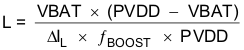
ΔIL is inversely proportional to L. Minimize ΔIL as much as is necessary for a specific application. Increase the inductance to reduce the ripple current. Do not use greater than 4.7 μH, as this prevents the boost converter from responding to fast output current changes properly. If using above 3.3 µH, then use at least 10 µF capacitance on PVOUT to ensure boost converter stability.
The typical inductor value range for the TPA2015D1 is 2.2 μH to 3.3 µH. Select an inductor with less than 0.5 Ω dc resistance, DCR. Higher DCR reduces total efficiency due to an increase in voltage drop across the inductor.
| L (μH) | SUPPLIER | COMPONENT CODE | SIZE (L×W×H mm) | DCR TYP (mΩ) | ISAT MAX (A) | C RANGE |
|---|---|---|---|---|---|---|
| 2.2 | Chilisin Electronics Corp. | CLCN252012T-2R2M-N | 2.5 x 2.0 x 1.2 | 105 | 1.2 | 4.7 – 22 µF / 16 V 6.8 – 22 µF / 10 V |
| 2.2 | Toko | 1239AS-H-2R2N=P2 | 2.5 × 2.0 × 1.2 | 96 | 2.3 | |
| 2.2 | Coilcraft | XFL4020-222MEC | 4.0 x 4.0 x 2.15 | 22 | 3.5 | |
| 3.3 | Toko | 1239AS-H-3R3N=P2 | 2.5 × 2.0 × 1.2 | 160 | 2.0 | 10 – 22 µF / 10 V |
| 3.3 | Coilcraft | XFL4020-332MEC | 4.0 x 4.0 x 2.15 | 35 | 2.8 |