ZHCSQQ4C November   2011  – June 2022 TPA2015D1

PRODUCTION DATA  

  1. 特性
  2. 应用
  3. 说明
  4. Revision History
  5. Device Comparison Table
  6. Pin Configuration and Functions
  7. Specifications
    1. 7.1 Absolute Maximum Ratings
    2. 7.2 ESD Ratings
    3. 7.3 Recommended Operating Conditions
    4. 7.4 Thermal Information
    5. 7.5 Electrical Characteristics
    6. 7.6 Operating Characteristics
    7. 7.7 Typical Characteristics
  8. Parameter Measurement Information
  9. Detailed Description
    1. 9.1 Overview
    2. 9.2 Functional Block Diagram
    3. 9.3 Feature Description
      1. 9.3.1 SpeakerGuard™ Theory of Operation
        1. 9.3.1.1 SpeakerGuard™ With Varying Input Levels
        2. 9.3.1.2 Battery Tracking SpeakerGuard™
      2. 9.3.2 Fully Differential Class-D Amplifier
        1. 9.3.2.1 Advantages of Fully Differential Amplifiers
        2. 9.3.2.2 Improved Class-D Efficiency
      3. 9.3.3 Adaptive Boost Converter
        1. 9.3.3.1 Boost Converter Overvoltage Protection
      4. 9.3.4 Operation With DACs and CODECs
      5. 9.3.5 Filter Free Operation and Ferrite Bead Filters
      6. 9.3.6 Speaker Load Limitation
      7. 9.3.7 Fixed Gain Setting
    4. 9.4 Device Functional Modes
      1. 9.4.1 Shutdown Mode
      2. 9.4.2 Battery Tracking SpeakerGuard™ Operation
  10. 10Application and Implementation
    1. 10.1 Application Information
    2. 10.2 Typical Applications
      1. 10.2.1 TPA2015D1 With Differential Input Signals
        1. 10.2.1.1 Design Requirements
        2. 10.2.1.2 Detailed Design Procedure
          1. 10.2.1.2.1 Boost Converter Inductor Selection
            1. 10.2.1.2.1.1 Inductor Equations
          2. 10.2.1.2.2 Boost Converter Capacitor Selection
          3. 10.2.1.2.3 Components Location and Selection
            1. 10.2.1.2.3.1 Decoupling Capacitors
            2. 10.2.1.2.3.2 Input Capacitors
        3. 10.2.1.3 Application Curves
      2. 10.2.2 TPA2015D1 with Single-Ended Input Signals
        1. 10.2.2.1 Design Requirements
        2. 10.2.2.2 Detailed Design Procedure
        3. 10.2.2.3 Application Curves
  11. 11Power Supply Recommendations
    1. 11.1 Power Supply Decoupling Capacitors
  12. 12Layout
    1. 12.1 Layout Guidelines
      1. 12.1.1 Component Placement
      2. 12.1.2 Trace Width
      3. 12.1.3 Pad Size
    2. 12.2 Layout Example
  13. 13Device and Documentation Support
    1. 13.1 Device Support
      1. 13.1.1 Device Nomenclature
        1. 13.1.1.1 TPA2015D1 Glossary
        2. 13.1.1.2 Boost Terms
    2. 13.2 Community Resources
    3. 13.3 Trademarks
  14. 14Mechanical, Packaging, and Orderable Information
    1. 14.1 Package Option Addendum
      1. 14.1.1 Packaging Information
      2. 14.1.2 Tape and Reel Information

封装选项

机械数据 (封装 | 引脚)
散热焊盘机械数据 (封装 | 引脚)
订购信息
Boost Converter Capacitor Selection

The value of the boost capacitor is determined by the minimum value of working capacitance required for stability and the maximum voltage ripple allowed on PVDD in the application. Working capacitance refers to the available capacitance after derating the capacitor value for DC bias, temperature, and aging.

Do not use any component with a working capacitance less than 4.7 μF. This corresponds to a 4.7 µF / 16 V capacitor, or a 6.8 µF / 10 V capacitor. Do not use above 22 µF capacitance as it will reduce the boost converter response time to large output current transients.

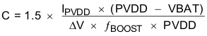
Equation 3 shows the relationship between the boost capacitance, C, to load current, load voltage, ripple voltage, input voltage, and switching frequency (IPVDD, PVDD, ΔV, VBAT, and fBOOST respectively).

Insert the maximum allowed ripple voltage into Equation 3 and solve for C. The 1.5 multiplier accounts for capacitance loss due to applied dc voltage and temperature for X5R and X7R ceramic capacitors.

Equation 3. GUID-F8261707-198F-41DA-AC04-414CD5E8C0B9-low.gif