ZHCSIE4A June 2018 – July 2018 TMS320F28035-EP
PRODUCTION DATA.
- 1器件概述
- 2修订历史记录
- 3Terminal Configuration and Functions
-
4Specifications
- 4.1 Absolute Maximum Ratings
- 4.2 ESD Ratings
- 4.3 Power-On Hours (POH) Limits
- 4.4 Recommended Operating Conditions
- 4.5 Power Consumption Summary
- 4.6 Electrical Characteristics
- 4.7 Thermal Resistance Characteristics
- 4.8 Thermal Design Considerations
- 4.9 Emulator Connection Without Signal Buffering for the MCU
- 4.10 Parameter Information
- 4.11 Test Load Circuit
- 4.12 Power Sequencing
- 4.13 Clock Specifications
- 4.14 Flash Timing
-
5Detailed Description
- 5.1
Overview
- 5.1.1 CPU
- 5.1.2 Control Law Accelerator (CLA)
- 5.1.3 Memory Bus (Harvard Bus Architecture)
- 5.1.4 Peripheral Bus
- 5.1.5 Real-Time JTAG and Analysis
- 5.1.6 Flash
- 5.1.7 M0, M1 SARAMs
- 5.1.8 L0 SARAM, and L1, L2, and L3 DPSARAMs
- 5.1.9 Boot ROM
- 5.1.10 Security
- 5.1.11 Peripheral Interrupt Expansion (PIE) Block
- 5.1.12 External Interrupts (XINT1–XINT3)
- 5.1.13 Internal Zero Pin Oscillators, Oscillator, and PLL
- 5.1.14 Watchdog
- 5.1.15 Peripheral Clocking
- 5.1.16 Low-power Modes
- 5.1.17 Peripheral Frames 0, 1, 2, 3 (PFn)
- 5.1.18 General-Purpose Input/Output (GPIO) Multiplexer
- 5.1.19 32-Bit CPU-Timers (0, 1, 2)
- 5.1.20 Control Peripherals
- 5.1.21 Serial Port Peripherals
- 5.2 Memory Maps
- 5.3 Register Maps
- 5.4 Device Emulation Registers
- 5.5 VREG/BOR/POR
- 5.6 System Control
- 5.7 Low-Power Modes Block
- 5.8 Interrupts
- 5.9
Peripherals
- 5.9.1 Control Law Accelerator (CLA) Overview
- 5.9.2 Analog Block
- 5.9.3 Detailed Descriptions
- 5.9.4 Serial Peripheral Interface (SPI) Module
- 5.9.5 Serial Communications Interface (SCI) Module
- 5.9.6 Local Interconnect Network (LIN)
- 5.9.7 Enhanced Controller Area Network (eCAN) Module
- 5.9.8 Inter-Integrated Circuit (I2C)
- 5.9.9 Enhanced PWM Modules (ePWM1/2/3/4/5/6/7)
- 5.9.10 High-Resolution PWM (HRPWM)
- 5.9.11 Enhanced Capture Module (eCAP1)
- 5.9.12 High-Resolution Capture (HRCAP) Module
- 5.9.13 Enhanced Quadrature Encoder Pulse (eQEP)
- 5.9.14 JTAG Port
- 5.9.15 General-Purpose Input/Output (GPIO) MUX
- 5.1
Overview
- 6Applications, Implementation, and Layout
- 7器件和文档支持
- 8机械、封装和可订购信息
5.9.7 Enhanced Controller Area Network (eCAN) Module
The CAN module (eCAN-A) has the following features:
- Fully compliant with ISO11898-1 (CAN 2.0B)
- Supports data rates up to 1 Mbps
- Thirty-two mailboxes, each with the following properties:
- Configurable as receive or transmit
- Configurable with standard or extended identifier
- Has a programmable receive mask
- Supports data and remote frame
- Composed of 0 to 8 bytes of data
- Uses a 32-bit time stamp on receive and transmit message
- Protects against reception of new message
- Holds the dynamically programmable priority of transmit message
- Employs a programmable interrupt scheme with two interrupt levels
- Employs a programmable alarm on transmission or reception time-out
- Low-power mode
- Programmable wake-up on bus activity
- Automatic reply to a remote request message
- Automatic retransmission of a frame in case of loss of arbitration or error
- 32-bit local network time counter synchronized by a specific message (communication in conjunction with mailbox 16)
- Self-test mode
- Operates in a loopback mode receiving its own message. A "dummy" acknowledge is provided, thereby eliminating the need for another node to provide the acknowledge bit.
NOTE
For a SYSCLKOUT of 60 MHz, the smallest bit rate possible is 4.6875 kbps.
The F2803x CAN has passed the conformance test per ISO/DIS 16845. Contact TI for test report and exceptions.
For information on using the CAN module with the on-chip zero-pin oscillators, see Piccolo MCU CAN Module Operation Using the On-Chip Zero-Pin Oscillator.
For more information on the CAN, see the TMS320x2803x Piccolo Enhanced Controller Area Network (eCAN) Reference Guide.
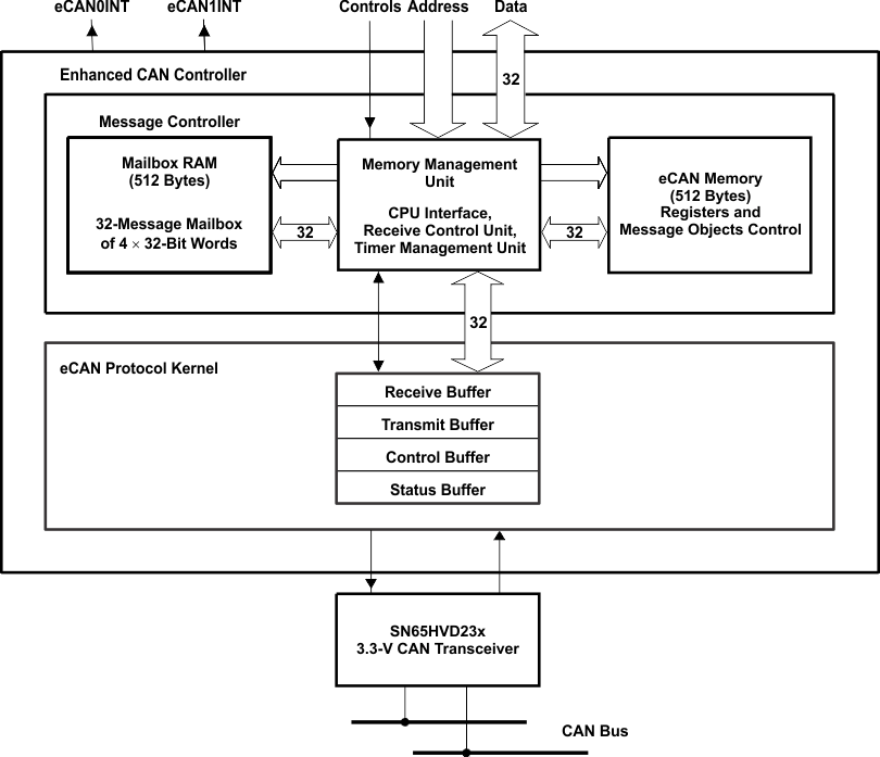
 Figure 5-32 eCAN Block Diagram and Interface Circuit
 Table 5-41 3.3-V eCAN Transceivers
| PART NUMBER | SUPPLY
VOLTAGE |
LOW-POWER
MODE |
SLOPE
CONTROL |
VREF | OTHER | TA |
|---|---|---|---|---|---|---|
| SN65HVD230 | 3.3 V | Standby | Adjustable | Yes | – | –40°C to 85°C |
| SN65HVD230Q | 3.3 V | Standby | Adjustable | Yes | – | –40°C to 125°C |
| SN65HVD231 | 3.3 V | Sleep | Adjustable | Yes | – | –40°C to 85°C |
| SN65HVD231Q | 3.3 V | Sleep | Adjustable | Yes | – | –40°C to 125°C |
| SN65HVD232 | 3.3 V | None | None | None | – | –40°C to 85°C |
| SN65HVD232Q | 3.3 V | None | None | None | – | –40°C to 125°C |
| SN65HVD233 | 3.3 V | Standby | Adjustable | None | Diagnostic Loopback | –40°C to 125°C |
| SN65HVD234 | 3.3 V | Standby and Sleep | Adjustable | None | – | –40°C to 125°C |
| SN65HVD235 | 3.3 V | Standby | Adjustable | None | Autobaud Loopback | –40°C to 125°C |
| ISO1050 | 3–5.5 V | None | None | None | Built-in Isolation
Low Prop Delay Thermal Shutdown Failsafe Operation Dominant Time-Out |
–55°C to 105°C |
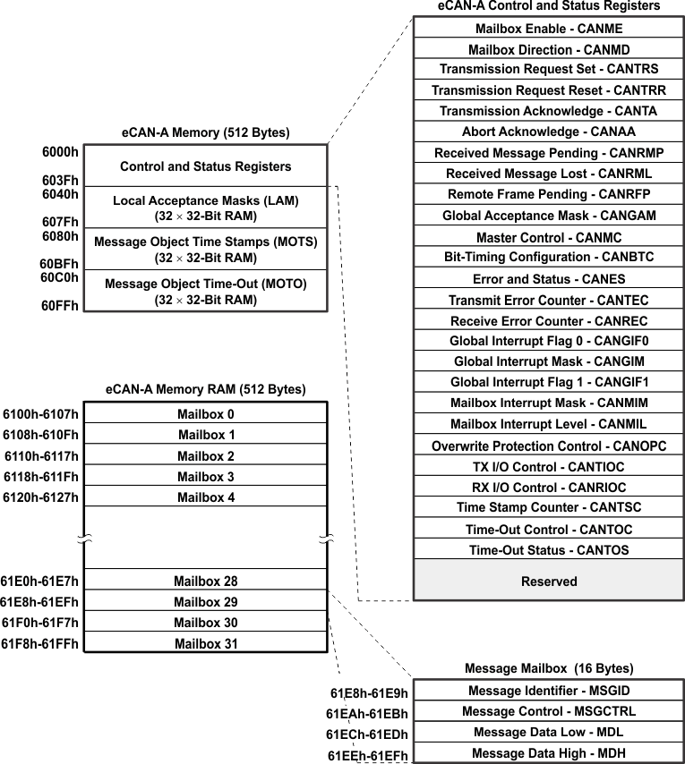
 Figure 5-33 eCAN-A Memory Map
 NOTE
If the eCAN module is not used in an application, the RAM available (LAM, MOTS, MOTO, and mailbox RAM) can be used as general-purpose RAM. The CAN module clock should be enabled for this.
The CAN registers listed in Table 5-42 are used by the CPU to configure and control the CAN controller and the message objects. eCAN control registers only support 32-bit read/write operations. Mailbox RAM can be accessed as 16 bits or 32 bits. 32-bit accesses are aligned to an even boundary.
Table 5-42 CAN Register Map(1)
| REGISTER NAME | eCAN-A
ADDRESS |
SIZE (x32) | DESCRIPTION | ||
|---|---|---|---|---|---|
| CANME | 0x6000 | 1 | Mailbox enable | ||
| CANMD | 0x6002 | 1 | Mailbox direction | ||
| CANTRS | 0x6004 | 1 | Transmit request set | ||
| CANTRR | 0x6006 | 1 | Transmit request reset | ||
| CANTA | 0x6008 | 1 | Transmission acknowledge | ||
| CANAA | 0x600A | 1 | Abort acknowledge | ||
| CANRMP | 0x600C | 1 | Receive message pending | ||
| CANRML | 0x600E | 1 | Receive message lost | ||
| CANRFP | 0x6010 | 1 | Remote frame pending | ||
| CANGAM | 0x6012 | 1 | Global acceptance mask | ||
| CANMC | 0x6014 | 1 | Master control | ||
| CANBTC | 0x6016 | 1 | Bit-timing configuration | ||
| CANES | 0x6018 | 1 | Error and status | ||
| CANTEC | 0x601A | 1 | Transmit error counter | ||
| CANREC | 0x601C | 1 | Receive error counter | ||
| CANGIF0 | 0x601E | 1 | Global interrupt flag 0 | ||
| CANGIM | 0x6020 | 1 | Global interrupt mask | ||
| CANGIF1 | 0x6022 | 1 | Global interrupt flag 1 | ||
| CANMIM | 0x6024 | 1 | Mailbox interrupt mask | ||
| CANMIL | 0x6026 | 1 | Mailbox interrupt level | ||
| CANOPC | 0x6028 | 1 | Overwrite protection control | ||
| CANTIOC | 0x602A | 1 | TX I/O control | ||
| CANRIOC | 0x602C | 1 | RX I/O control | ||
| CANTSC | 0x602E | 1 | Time stamp counter (Reserved in SCC mode) | ||
| CANTOC | 0x6030 | 1 | Time-out control (Reserved in SCC mode) | ||
| CANTOS | 0x6032 | 1 | Time-out status (Reserved in SCC mode) | ||