ZHCSA13P November 2008 – February 2021 TMS320F28020 , TMS320F280200 , TMS320F28021 , TMS320F28022 , TMS320F28023 , TMS320F28023-Q1 , TMS320F28026 , TMS320F28026-Q1 , TMS320F28026F , TMS320F28027 , TMS320F28027-Q1 , TMS320F28027F , TMS320F28027F-Q1
PRODUCTION DATA
- 1 特性
- 2 应用
- 3 说明
- 4 功能方框图
- 5 修订历史记录
- 6 Device Comparison
- 7 Terminal Configuration and Functions
- 8 规格
-
9 详细说明
- 9.1
Overview
- 9.1.1 CPU
- 9.1.2 Memory Bus (Harvard Bus Architecture)
- 9.1.3 外设总线
- 9.1.4 Real-Time JTAG and Analysis
- 9.1.5 Flash
- 9.1.6 M0,M1 SARAM
- 9.1.7 L0 SARAM
- 9.1.8 Boot ROM
- 9.1.9 Security
- 9.1.10 外设中断扩展 (PIE) 块
- 9.1.11 外部中断 (XINT1-XINT3)
- 9.1.12 内部零引脚振荡器、振荡器和 PLL
- 9.1.13 看门狗
- 9.1.14 Peripheral Clocking
- 9.1.15 Low-power Modes
- 9.1.16 外设帧 0,1,2 (PFn)
- 9.1.17 通用输入/输出 (GPIO) 复用器
- 9.1.18 32 位 CPU 定时器 (0,1,2)
- 9.1.19 Control Peripherals
- 9.1.20 串行端口外设
- 9.2 Memory Maps
- 9.3 Register Maps
- 9.4 Device Emulation Registers
- 9.5 VREG/BOR/POR
- 9.6 系统控制
- 9.7 Low-power Modes Block
- 9.8 Interrupts
- 9.9
外设
- 9.9.1 Analog Block
- 9.9.2 详细说明
- 9.9.3 Serial Peripheral Interface (SPI) Module
- 9.9.4 Serial Communications Interface (SCI) Module
- 9.9.5 Inter-Integrated Circuit (I2C)
- 9.9.6 Enhanced PWM Modules (ePWM1/2/3/4)
- 9.9.7 High-Resolution PWM (HRPWM)
- 9.9.8 Enhanced Capture Module (eCAP1)
- 9.9.9 JTAG 端口
- 9.9.10 General-Purpose Input/Output (GPIO) MUX
- 9.1
Overview
- 10应用、实施和布局
- 11器件和文档支持
- 12机械、封装和可订购信息
封装选项
机械数据 (封装 | 引脚)
散热焊盘机械数据 (封装 | 引脚)
- DA|38
订购信息
9.9.3 Serial Peripheral Interface (SPI) Module
The device includes the four-pin serial peripheral interface (SPI) module. One SPI module (SPI-A) is available. The SPI is a high-speed, synchronous serial I/O port that allows a serial bit stream of programmed length (1 to 16 bits) to be shifted into and out of the device at a programmable bit-transfer rate. Normally, the SPI is used for communications between the MCU and external peripherals or another processor. Typical applications include external I/O or peripheral expansion through devices such as shift registers, display drivers, and ADCs. Multidevice communications are supported by the master/slave operation of the SPI.
The SPI module features include:
- Four external pins:
- SPISOMI: SPI slave-output/master-input pin
- SPISIMO: SPI slave-input/master-output pin
- SPISTE: SPI slave transmit-enable pin
- SPICLK: SPI serial-clock pin
All four pins can be used as GPIO if the SPI module is not used.
- Two operational modes: master and slave
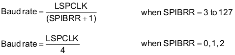
Baud rate: 125 different programmable rates.
- Data word length: 1 to 16 data bits
- Four clocking schemes (controlled by clock polarity and clock phase bits) include:
- Falling edge without phase delay: SPICLK active-high. SPI transmits data on the falling edge of the SPICLK signal and receives data on the rising edge of the SPICLK signal.
- Falling edge with phase delay: SPICLK active-high. SPI transmits data one half-cycle ahead of the falling edge of the SPICLK signal and receives data on the falling edge of the SPICLK signal.
- Rising edge without phase delay: SPICLK inactive-low. SPI transmits data on the rising edge of the SPICLK signal and receives data on the falling edge of the SPICLK signal.
- Rising edge with phase delay: SPICLK inactive-low. SPI transmits data one half-cycle ahead of the rising edge of the SPICLK signal and receives data on the rising edge of the SPICLK signal.
- Simultaneous receive and transmit operation (transmit function can be disabled in software)
- Transmitter and receiver operations are accomplished through either interrupt-driven or polled algorithms.
- Nine SPI module control registers: In control register frame beginning at address 7040h.
Note:
All registers in this module are 16-bit registers that are connected to Peripheral Frame 2. When a register is accessed, the register data is in the lower byte (7–0), and the upper byte (15–8) is read as zeros. Writing to the upper byte has no effect.
Enhanced feature:
- 4-level transmit/receive FIFO
- Delayed transmit control
- Bidirectional 3 wire SPI mode support
The SPI port operation is configured and controlled by the registers listed in Table 9-24 .
| NAME | ADDRESS | SIZE (x16) | EALLOW PROTECTED | DESCRIPTION(1) |
|---|---|---|---|---|
| SPICCR | 0x7040 | 1 | No | SPI-A Configuration Control Register |
| SPICTL | 0x7041 | 1 | No | SPI-A Operation Control Register |
| SPISTS | 0x7042 | 1 | No | SPI-A Status Register |
| SPIBRR | 0x7044 | 1 | No | SPI-A Baud Rate Register |
| SPIRXEMU | 0x7046 | 1 | No | SPI-A Receive Emulation Buffer Register |
| SPIRXBUF | 0x7047 | 1 | No | SPI-A Serial Input Buffer Register |
| SPITXBUF | 0x7048 | 1 | No | SPI-A Serial Output Buffer Register |
| SPIDAT | 0x7049 | 1 | No | SPI-A Serial Data Register |
| SPIFFTX | 0x704A | 1 | No | SPI-A FIFO Transmit Register |
| SPIFFRX | 0x704B | 1 | No | SPI-A FIFO Receive Register |
| SPIFFCT | 0x704C | 1 | No | SPI-A FIFO Control Register |
| SPIPRI | 0x704F | 1 | No | SPI-A Priority Control Register |
For more information on the SPI, see the Serial Peripheral Interface (SPI) chapter in the TMS320F2802x,TMS320F2802xx Technical Reference Manual.
Figure 9-28 is a block diagram of the SPI in slave mode.
")