ZHCSMZ5D April 2020 – January 2023 TLV841
PRODUCTION DATA
- 1 特性
- 2 应用
- 3 说明
- 4 Revision History
- 5 Device Comparison
- 6 Pin Configuration and Functions
- 7 Specifications
- 8 Detailed Description
- 9 Application and Implementation
- 10Power Supply Recommendations
- 11Layout
- 12Device and Documentation Support
- 13Mechanical, Packaging, and Orderable Information
8.3.3 User-Programmable Reset Time Delay for TLV841C only
The reset time delay can be set to a typical value of 40 µs by leaving the CT pin floating, or a maximum value of approximately 6.2 seconds by connecting 10 µF delay capacitor. The reset time delay (tD) can be programmed by connecting a capacitor no larger than 10 µF between the CT pin and GND.
The relationship between external capacitor (CCT_EXT (typ)) in µF at CT pin and the time delay (tD (typ)) in seconds is given by #SNVSBC358016.
#SNVSBC358016 is simplified to #T5037184-33 by plugging RCT (typ) and tD (no cap, typ) given in GUID-XXXXXXXX-SF0T-XXXX-XXXX-000000182866.html#GUID-XXXXXXXX-SF0T-XXXX-XXXX-000000182866 and GUID-XXXXXXXX-SF0T-XXXX-XXXX-000000182867.html#GUID-XXXXXXXX-SF0T-XXXX-XXXX-000000182867:
#T5037184-34 solves for external capacitor value CCT_EXT in units of µF where tD (typ) is in units of seconds
The recommended maximum delay capacitor for the TLV841C is limited to 10 μF as this ensures enough time for the capacitor to fully discharge when a voltage fault occurs. Also, having a too large of a capacitor value can cause very slow charge up (rise times) and system noise can cause the the internal circuit to trip earlier or later near the threshold. This leads to variation in time delay where it can make the delay accuracy worse in the presence of system noise.
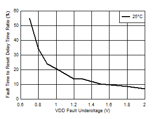
When a voltage fault occurs, the previously charged up capacitor discharges and if the monitored voltage returns from the fault condition before the delay capacitor discharges completely, the delay will be shorter than expected. The capacitor will begin charging from a voltage above zero and resulting in shorter than expected time delay. A larger delay capacitor can be used so long as the capacitor has enough time to fully discharge during the duration of the voltage fault. The amount of time required to discharge the delay capacitor relative to the reset delay rises as VDD fault undervoltage increases as shown in #T5753602-4. From the graph below, to ensure the CCT_EXT capacitor is fully discharged, the time period or duration of the voltage fault needs to be greater than 10% of the programmed reset time delay.
 Figure 8-5 CCT_EXT Discharge
Time During Fault Condition (CCT_EXT = 1 µF)