ZHCSUT0D October 2001 – February 2024 TFP410
PRODUCTION DATA
- 1
- 1 特性
- 2 应用
- 3 说明
- 4 Pin Configuration and Functions
- 5 Specifications
-
6 Detailed Description
- 6.1 Overview
- 6.2 Functional Block Diagram
- 6.3 Feature Description
- 6.4 Device Functional Modes
- 6.5 Programming
- 6.6
Register Maps
- 6.6.1 VEN_ID Register (Sub-Address = 01−00 ) [reset = 0x014C]
- 6.6.2 DEV_ID Register (Sub-Address = 03–02) [reset = 0x0410]
- 6.6.3 REV_ID Register (Sub-Address = 04) [reset = 0x00]
- 6.6.4 Reserved Register (Sub-Address = 07–05) [reset = 0x641400]
- 6.6.5 CTL_1_MODE (Sub-Address = 08) [reset = 0xBE]
- 6.6.6 CTL_2_MODE Register (Sub-Address = 09) [reset = 0x00]
- 6.6.7 CTL_3_MODE Register (Sub-Address = 0A) [reset = 0x80]
- 6.6.8 CFG Register (Sub-Address = 0B)
- 6.6.9 RESERVED Register (Sub-Address = 0E–0C) [reset = 0x97D0A9]
- 6.6.10 DE_DLY Register (Sub-Address = 32) [reset = 0x00]
- 6.6.11 DE_CTL Register (Sub-Address = 33) [reset = 0x00]
- 6.6.12 DE_TOP Register (Sub-Address = 34) [reset = 0x00]
- 6.6.13 DE_CNT Register (Sub-Address = 37–36) [reset = 0x0000]
- 6.6.14 DE_LIN Register (Sub-Address = 39–38) [reset = 0x0000]
- 6.6.15 H_RES Register (Sub-Address = 3B−3A)
- 6.6.16 V_RES Register (Sub-Address = 3D−3C)
- 7 Application and Implementation
- 8 Device and Documentation Support
- 9 Revision History
- 10Mechanical, Packaging, and Orderable Information
封装选项
请参考 PDF 数据表获取器件具体的封装图。
机械数据 (封装 | 引脚)
- PAP|64
散热焊盘机械数据 (封装 | 引脚)
- PAP|64
订购信息
6.5.1 I2C Interface
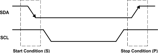
The I2C interface is used to access the internal TFP410 registers. This two-pin interface consists of the SCL clock line and the SDA serial data line. The basic I2C access cycles are shown in Figure 6-5 and Figure 6-6.
 Figure 6-5 I2C Start and Stop Conditions
The basic access write cycle consists of the following:
- A start condition
- A target address cycle
- A sub-address cycle
- Any number of data cycles
- A stop condition
The basic access read cycle consists of the following:
- A start condition
- A target write address cycle
- A sub-address cycle
- A restart condition
- A target read address cycle
- Any number of data cycles
- A stop condition
The start and stop conditions are shown in Figure 6-5. The high to low transition of SDA while SCL is high defines the start condition. The low to high transition of SDA while SCL is high defines the stop condition. Each cycle, data or address, consists of 8 bits of serial data followed by one acknowledge bit generated by the receiving device. Thus, each data/address cycle contains 9 bits as shown in Figure 6-6.
 Figure 6-6 I2C Access Cycles
Following a start condition, each I2C device decodes the target address. The TFP410 responds with an acknowledge by pulling the SDA line low during the ninth clock cycle if it decodes the address as its address. During subsequent sub-address and data cycles, the TFP410 responds with acknowledge as shown in Figure 6-7. The sub-address is auto-incremented after each data cycle.
The transmitting device must not drive the SDA signal during the acknowledge cycle so that the receiving device may drive the SDA signal low. The controller indicates a not acknowledge condition ( A) by keeping the SDA signal high just before it asserts the stop condition (P). This sequence terminates a read cycle as shown in Figure 6-8.
The target address consists of 7 bits of address along with 1 bit of read/write information (read = 1, write = 0) as shown below in Figure 6-6 and Figure 6-7. For the TFP410, the selectable target addresses (including the R/W bit) using A[3:1] are 0x70, 0x72, 0x74, 0x76, 0x78, 0x7A, 0x7C, and 0x7E for write cycles and 0x71, 0x73, 0x75, 0x77, 0x79, 0x7B, 0x7D, and 0x7F for read cycles.
 Figure 6-7 I2C Write Cycle
 Figure 6-8 I2C Read Cycle