ZHCSUT0D October 2001 – February 2024 TFP410
PRODUCTION DATA
- 1
- 1 特性
- 2 应用
- 3 说明
- 4 Pin Configuration and Functions
- 5 Specifications
-
6 Detailed Description
- 6.1 Overview
- 6.2 Functional Block Diagram
- 6.3 Feature Description
- 6.4 Device Functional Modes
- 6.5 Programming
- 6.6
Register Maps
- 6.6.1 VEN_ID Register (Sub-Address = 01−00 ) [reset = 0x014C]
- 6.6.2 DEV_ID Register (Sub-Address = 03–02) [reset = 0x0410]
- 6.6.3 REV_ID Register (Sub-Address = 04) [reset = 0x00]
- 6.6.4 Reserved Register (Sub-Address = 07–05) [reset = 0x641400]
- 6.6.5 CTL_1_MODE (Sub-Address = 08) [reset = 0xBE]
- 6.6.6 CTL_2_MODE Register (Sub-Address = 09) [reset = 0x00]
- 6.6.7 CTL_3_MODE Register (Sub-Address = 0A) [reset = 0x80]
- 6.6.8 CFG Register (Sub-Address = 0B)
- 6.6.9 RESERVED Register (Sub-Address = 0E–0C) [reset = 0x97D0A9]
- 6.6.10 DE_DLY Register (Sub-Address = 32) [reset = 0x00]
- 6.6.11 DE_CTL Register (Sub-Address = 33) [reset = 0x00]
- 6.6.12 DE_TOP Register (Sub-Address = 34) [reset = 0x00]
- 6.6.13 DE_CNT Register (Sub-Address = 37–36) [reset = 0x0000]
- 6.6.14 DE_LIN Register (Sub-Address = 39–38) [reset = 0x0000]
- 6.6.15 H_RES Register (Sub-Address = 3B−3A)
- 6.6.16 V_RES Register (Sub-Address = 3D−3C)
- 7 Application and Implementation
- 8 Device and Documentation Support
- 9 Revision History
- 10Mechanical, Packaging, and Orderable Information
封装选项
请参考 PDF 数据表获取器件具体的封装图。
机械数据 (封装 | 引脚)
- PAP|64
散热焊盘机械数据 (封装 | 引脚)
- PAP|64
订购信息
5.6 Timing Requirements
| MIN | NOM | MAX | UNIT | |||
|---|---|---|---|---|---|---|
| t(pixel) | Pixel time period(1) | 6.06 | 40 | ns | ||
| t(IDCK) | IDCK duty cycle | 30% | 70% | |||
| t(ijit) | IDCK clock jitter tolerance | 2 | ns | |||
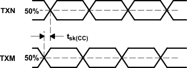
| tsk(CC) | DVI output inter-pair or channel-to-channel skew (2), see Figure 5-2 | f(IDCK) = 165MHz | 1.2 | ns | ||
| tsu(IDF) | Data, DE, VSYNC, HSYNC setup time to IDCK+ falling edge, see Figure 5-2 | Single edge (BSEL=1, DSEL=0, DKEN=0, EDGE=0) | 1.2 | ns | ||
| th(IDF) | Data, DE, VSYNC, HSYNC hold time to IDCK+ falling edge, see Figure 5-2 | 1.3 | ns | |||
| tsu(IDR) | Data, DE, VSYNC, HSYNC setup time to IDCK+ rising edge, see Figure 5-2 | Single edge (BSEL=1, DSEL=0, DKEN=0, EDGE=1) | 1.2 | ns | ||
| th(IDR) | Data, DE, VSYNC, HSYNC hold time to IDCK+ rising edge, see Figure 5-2 | 1.3 | ns | |||
| tsu(ID) | Data, DE, VSYNC, HSYNC setup time to IDCK+ falling/rising edge, see Figure 5-3 | Dual edge(BSEL=0, DSEL=1, DKEN=0) | 0.9 | ns | ||
| th(ID) | Data, DE, VSYNC, HSYNC hold time to IDCK+ falling/rising edge, see Figure 5-3 | Dual edge (BSEL=0, DSEL=1, DKEN=0) | 1 | ns | ||
(1) t(pixel) is the pixel time defined as the period of the TXC output clock. The period of IDCK is equal to t(pixel).
(2) Measured differentially at the 50% crossing point using the IDCK+ input clock as a trigger.
 Figure 5-1 Rise and Fall Time for DVI Outputs
 Figure 5-2 Control and Single-Edge-Data Setup/Hold Time to IDCK±
 Figure 5-3 Dual Edge Data Setup/Hold Times to IDCK+
 Figure 5-4 Analog Output Intra-Pair ± Differential Skew
 Figure 5-5 Analog Output Channel-to-Channel Skew