ZHCSVD3E December 2003 – March 2024 SN65MLVD200A , SN65MLVD202A , SN65MLVD204A , SN65MLVD205A
PRODUCTION DATA
9.2.2.2 电源旁路电容
旁路电容器在配电电路中发挥着关键作用。在低频情况下,电源在其端子之间提供阻抗非常低的路径。但是,当更高频率的电流通过电源布线传播时,源极通常无法保持低阻抗的接地路径。旁路电容器用于克服这一缺点。通常,板级大旁路电容器(10μF 至 1000μF)可以很好地达到 kHz 范围。由于大电容器的引线大小和长度,它们在开关频率下往往具有较大的电感值。要解决这个问题,必须将较小的电容器(nF 至 μF 范围内)安装在本地集成电路旁边。
多层陶瓷芯片或表面贴装电容器(尺寸 0603 或 0805)可更大限度减少高速环境中旁路电容器的引线电感,因为它们的引线电感约为 1nH。为便于比较,带引线的典型电容器的引线电感约为 5nH。
根据 Howard Johnson 和 Martin Graham (1993) 所著的 High Speed Digital Design – A Handbook of Black Magic,在本地与 M-LVDS 芯片搭配使用的旁路电容值可由方程式 1 和方程式 2 确定。4ns 的保守上升时间和 100mA 在最坏情况下的电源电流变化涵盖了德州仪器 (TI) 提供的 M-LVDS 器件的整个范围。在此示例中,可容忍的最大电源噪声为 100mV;但是,该数字因设计中可用的噪声预算而异。
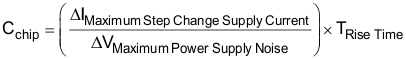

图 9-2 展示了一种可降低引线电感并涵盖板级电容器 (> 10µF) 与上述电容值 (0.004µF) 之间的中间频率的配置。将最小电容值放置在尽可能靠近芯片的位置。
 图 9-2 建议的 M-LVDS 旁路电容器布局