ZHCSLU2B December 2021 – October 2023 LM63460-Q1
PRODUCTION DATA
- 1
- 1 特性
- 2 应用
- 3 说明
- 4 Revision History
- 5 Device Comparison Table
- 6 Pin Configuration and Functions
- 7 Specifications
-
8 Detailed Description
- 8.1 Overview
- 8.2 Functional Block Diagram
- 8.3
Feature Description
- 8.3.1 Input Voltage Range (VIN1, VIN2)
- 8.3.2 Output Voltage Setpoint (FB)
- 8.3.3 Precision Enable and Input Voltage UVLO (EN/SYNC)
- 8.3.4 Frequency Synchronization (EN/SYNC)
- 8.3.5 Clock Locking
- 8.3.6 Adjustable Switching Frequency (RT)
- 8.3.7 Power-Good Monitor (PGOOD)
- 8.3.8 Bias Supply Regulator (VCC, BIAS)
- 8.3.9 Bootstrap Voltage and UVLO (CBOOT)
- 8.3.10 Spread Spectrum
- 8.3.11 Soft Start and Recovery From Dropout
- 8.3.12 Overcurrent and Short-Circuit Protection
- 8.3.13 Thermal Shutdown
- 8.3.14 Input Supply Current
- 8.4 Device Functional Modes
-
9 Application and Implementation
- 9.1 Application Information
- 9.2
Typical Applications
- 9.2.1
Design 1 – Automotive Synchronous Buck Regulator at 2.1 MHz
- 9.2.1.1 Design Requirements
- 9.2.1.2
Detailed Design Procedure
- 9.2.1.2.1 Custom Design With WEBENCH® Tools
- 9.2.1.2.2 Setting the Output Voltage
- 9.2.1.2.3 Choosing the Switching Frequency
- 9.2.1.2.4 Inductor Selection
- 9.2.1.2.5 Output Capacitor Selection
- 9.2.1.2.6 Input Capacitor Selection
- 9.2.1.2.7 Bootstrap Capacitor
- 9.2.1.2.8 VCC Capacitor
- 9.2.1.2.9 BIAS Power Connection
- 9.2.1.2.10 Feedforward Network
- 9.2.1.2.11 Input Voltage UVLO
- 9.2.1.3 Application Curves
- 9.2.2 Design 2 – Automotive Synchronous Buck Regulator at 400 kHz
- 9.2.1
Design 1 – Automotive Synchronous Buck Regulator at 2.1 MHz
- 9.3 Power Supply Recommendations
- 9.4 Layout
- 10Device and Documentation Support
- 11Mechanical, Packaging, and Orderable Information
9.3 Power Supply Recommendations
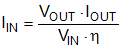
The characteristics of the input supply must be compatible with the Absolute Maximum Ratings and Recommended Operating Conditions in this data sheet. In addition, the input supply must be capable of delivering the required input current to the loaded converter. Estimate the average input current with Equation 15.
where
- η is the efficiency.
If the converter is connected to an input supply through long wires or PCB traces with a large impedance, take special care to achieve stable performance. The parasitic inductance and resistance of the input cables can have an adverse affect on converter operation. The parasitic inductance in combination with the low-ESR ceramic input capacitors form an underdamped resonant circuit, possibly resulting in instability and voltage transients each time the input supply is cycled ON and OFF. The parasitic resistance causes the input voltage to dip during a load transient. If the converter is operating close to the minimum input voltage, this dip can cause false UVLO triggering and a system reset.
The best way to solve such issues is to reduce the distance from the input supply to the converter and use an electrolytic input capacitor in parallel with the ceramics. The moderate ESR of the electrolytic capacitor helps damp the input resonant circuit and reduce any overshoot or undershoot at the input. A capacitance in the range of 47 μF to 100 μF is usually sufficient to provide input parallel damping and helps hold the input voltage steady during large load transients. An ESR of 0.1 Ω to 0.4 Ω provides enough damping for most input circuit configurations.
The input voltage must not be allowed to suddenly fall below the output voltage. In this scenario, such as a shorted input test, the output capacitors discharge through the body diode of the internal high-side power MOSFET. The current is effectively uncontrolled during this condition, possibly causing damage to the device. If this scenario is considered likely, then connect a Schottky bypass diode between the output and the input supply.