ZHCSMW2B December 2021 – December 2022 LM5123-Q1
PRODUCTION DATA
- 1 特性
- 2 应用
- 3 说明
- 4 Revision History
- 5 说明(续)
- 6 Pin Configuration and Functions
- 7 Specifications
-
8 Detailed Description
- 8.1 Overview
- 8.2 Functional Block Diagram
- 8.3
Feature Description
- 8.3.1 Device Enable/Disable (EN, VH Pin)
- 8.3.2 High Voltage VCC Regulator (BIAS, VCC Pin)
- 8.3.3 Light Load Switching Mode Selection (MODE Pin)
- 8.3.4 VOUT Range Selection (RANGE Pin)
- 8.3.5 Line Undervoltage Lockout (UVLO Pin)
- 8.3.6 Fast Restart using VCC HOLD (VH Pin)
- 8.3.7 Adjustable Output Regulation Target (VOUT, TRK, VREF Pin)
- 8.3.8 Overvoltage Protection (VOUT Pin)
- 8.3.9 Power Good Indicator (PGOOD Pin)
- 8.3.10 Dynamically Programmable Switching Frequency (RT)
- 8.3.11 External Clock Synchronization (SYNC Pin)
- 8.3.12 Programmable Spread Spectrum (DITHER Pin)
- 8.3.13 Programmable Soft Start (SS Pin)
- 8.3.14 Wide Bandwidth Transconductance Error Amplifier and PWM (TRK, COMP Pin)
- 8.3.15 Current Sensing and Slope Compensation (CSP, CSN Pin)
- 8.3.16 Constant Peak Current Limit (CSP, CSN Pin)
- 8.3.17 Maximum Duty Cycle and Minimum Controllable On-Time Limits
- 8.3.18 Deep Sleep Mode and Bypass Operation (HO, CP Pin)
- 8.3.19 MOSFET Drivers, Integrated Boot Diode, and Hiccup Mode Fault Protection (LO, HO, HB Pin)
- 8.3.20 Thermal Shutdown Protection
- 8.4 Device Functional Modes
- 9 Application and Implementation
- 10Power Supply Recommendations
- 11Layout
- 12Device and Documentation Support
- 13Mechanical, Packaging, and Orderable Information
8.3.13 Programmable Soft Start (SS Pin)
The soft-start feature helps the converter gradually reach the steady state operating point. To reduce start-up stresses and surges, the device regulates the error amplifier reference to the SS pin voltage or the TRK pin voltage (VTRK), whichever is lower.
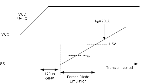
The internal 20 μA soft-start (ISS) current turns on 120 μs after the VCC pin crosses VVCC-UVLO. ISS gradually increases the voltage on an external soft-start capacitor (CSS). This results in a gradual rise of the output voltage.
In FPWM mode, the device forces diode emulation while the SS pin voltage is less than 1.5 V. When the SS pin voltage is greater than 1.5 V, the device changes the zero current detection (ZCD) threshold gradually from 4 mV to –145 mV to achieve a smooth transition from diode emulation to FPWM mode.
 Figure 8-12 Soft Start and Smooth Transition to
FPWM
Figure 8-12 Soft Start and Smooth Transition to
FPWMIn boost topology, the soft-start time (tSS) varies with the input supply voltage because the boost output voltage is equal to the boost input voltage at the beginning of the soft-start switching. tSS in boost topology is calculated in Equation 10.
In general, it is recommended to choose a soft-start time long enough so that the converter can start up without going into an overcurrent state. If the device is used for a pre-boost in automotive application, it is recommended to use 100-pF CSS to reach steady state as soon as possible.
The device also features an internal SS-to-FB clamp (VSS-FB), which clamps SS 55 mV above FB and is activated if 256 consecutive switching cycles occur with current limit. The SS-to-FB clamp is deactivated if 32 consecutive switching cycles occur without exceeding the current limit threshold. This clamp helps to minimize surges after output shorts or over load situations. The device can enter deep sleep mode when SS is greater than 1.5 V. It is not recommended to pulldown SS to stop switching.